A correlative approach combining TEM and SIMS for nanoscale quantification of dopant distributions in semiconductors
- Abstract number
- 496
- Event
- European Microscopy Congress 2020
- DOI
- 10.22443/rms.emc2020.496
- Corresponding Email
- [email protected]
- Session
- PSA.3 - Semiconductors & Devices
- Authors
- Dr. C.N. Shyam Kumar (1), Dr. Soupitak Pal (1), Dr. Tom Wirtz (1), Dr. Santhana Eswara (1)
- Affiliations
-
1. Advanced Instrumentation for Nano-Analytics (AINA), Materials Research and Technology Department, Luxembourg Institute of Science and Technology
- Keywords
Correlative microscopy, dopant distribution, secondary ion mass spectroscopy, transmission electron microscopy
- Abstract text
It is a well-known fact that the introduction of trace elements can greatly alter the physical and chemical properties of a material. This approach is widely used in the semiconductor industry and different kinds of dopants are used to tune the electronic properties of materials. In order to understand the effect of the dopants on the macroscopic electronic properties, it is imperative to have a quantitative nanoscale imaging of dopant concentrations down to ppm levels with high spatial resolutions.
High-resolution transmission electron microscope (HR-TEM) with different analytical capabilities can analyse materials with high spatial resolution, but detection and quantification of low atomic number elements and low concentrations is still a challenge. [1] On the other hand, secondary ion mass spectroscopy (SIMS) is a high-sensitivity analytical technique that can detect all elements down to ppm level but the lateral resolution is limited fundamentally because of the ion solid interaction volume. In addition, the quantification of SIMS intensities is not straight forward due to the difference in the ionisation yields and the matrix effect. [2] Thus, it is necessary to develop new correlative approaches for quantitative nanoscale analysis of very small concentration with high spatial resolutions. Here in this study, we make use of a novel approach combining TEM and SIMS for detection and quantification of very low dopant concentrations with high spatial resolutions.
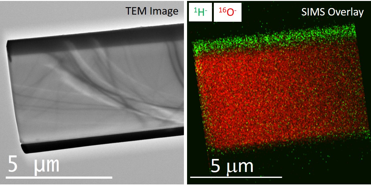
With in-situ and ex-situ correlative workflows involving TEM and SIMS, we look in to the dopant concentrations in carrier- selective passivating contacts in c-silicon solar cells. The set up consists of a modified Tecnai T20 attached with a Ga source FIB and an in-house developed compact mass spectrometer. This newly developed Parallel Ion Electron Spectrometry (PIES) can achieve correlative analysis by combining TEM and SIMS in a single instrument that enables detection of low Z elements with very low concentrations (figure 1).
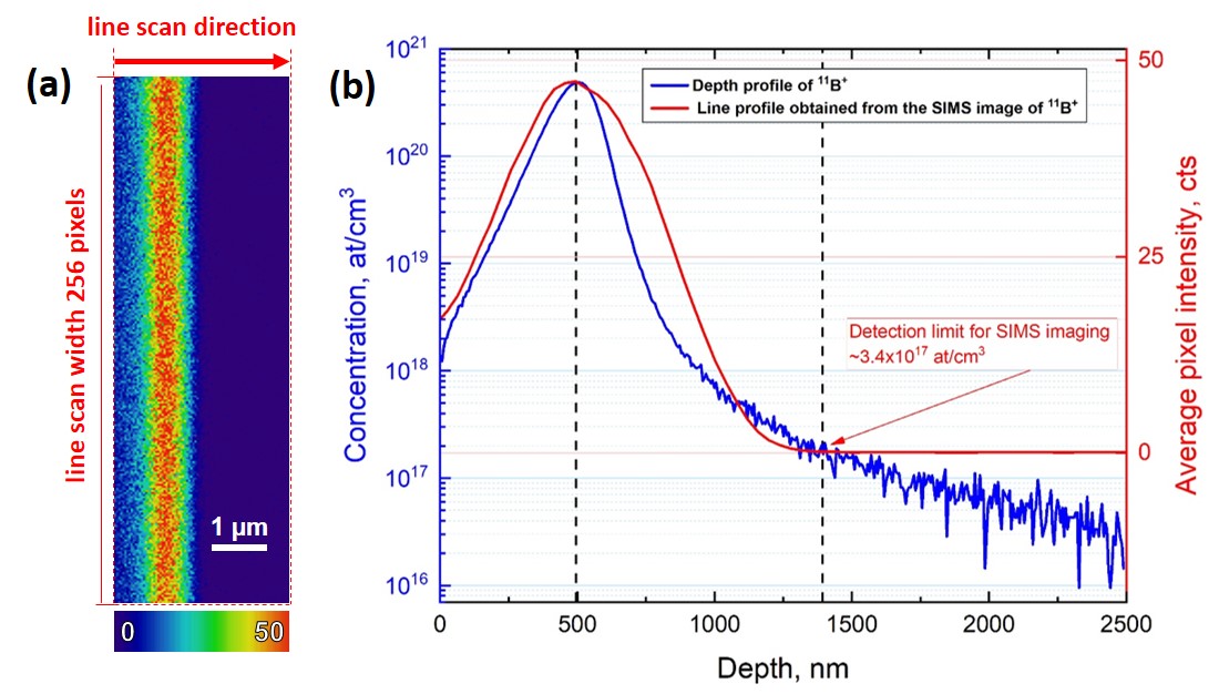
For the precise and rapid quantification of these images, we introduce a new method for direct quantitative SIMS imaging. The method is based on cross-sectional imaging of ion-implanted reference samples prepared using optimal ion dose and implantation energy. The cross sectional imaging enables the determination of reference concentrations varying continuously over few orders of magnitude with single image acquisition. [3] We demonstrate the quantification method using ex-situ SIMS imaging in a commercially available Cameca NanoSIMS50 instrument. Using O- primary ion beam with an impact energy of 16 keV, detection limit for boron in silicon was found to be ~3 × 10¹⁷ at./cm3 with a pixel size of 39 nm (figure 2).
By combining TEM and SIMS, the present approach opens up new opportunities for quantitative nanoscale analysis of very low-dopants concentration with high spatial resolutions in semiconductors. Complementary results from Atom Probe Tomography (APT) will also be presented to obtain a multi-scale perspective of variations in structure and chemical compositions.
Acknowledgments: This work is funded by FNR Luxembourg through the NACHOS project. The solar cell samples were fabricated by the team of Franz-Josef Haug and Aïcha Hessler-Wyser, PVLab, EPFL, Switzerland.
Figure 1: (a) TEM image of a cross-sectional FIB lamella of a thin-film solar cell deposited on an oxide substrate obtained from the PIES instrument and (b) overlay of 1H- and 16O- SIMS images from the same region. (Adapted from [2])
Figure 2: (a) Cross-sectional 11B+ SIMS image of the ion-implanted reference sample, (b) Boron distribution obtained by SIMS depth profiling (blue curve) and line scan intensity profile across the cross-section SIMS image (red curve). The line scan direction and the integration width used for averaging are indicated in (a). For the acquisition conditions here, the detection limit for the imaging SIMS is found to be ~3× 10¹⁷ at/cm3 with a pixel size of 39 nm. (Adapted from [3])
- References
[1] G. Botton and S. Prabhudev, “Analytical Electron Microscopy,” in Handbook of Microscopy. Springer Handbooks. Springer, Cham, 2019, pp. 2–2.
[2] S. Eswara et al., “Correlative microscopy combining transmission electron microscopy and secondary ion mass spectrometry: A general review on the state-of-the-art, recent developments, and prospects,” Appl. Phys. Rev., vol. 6, no. 2, p. 21312, Jun. 2019.
[3] S. Eswara et al., “A method for quantitative nanoscale imaging of dopant distributions using secondary ion mass spectrometry: an application example in silicon photovoltaics,” MRS Commun., vol. 9, no. 3, pp. 916–923, Sep. 2019.