A fully integrated in-situ solution for materials testing in SEM
- Abstract number
- 164
- Event
- European Microscopy Congress 2020
- DOI
- 10.22443/rms.emc2020.164
- Corresponding Email
- [email protected]
- Session
- PST.6 - In-situ and in-operando microscopy
- Authors
- Dr. Fang Zhou (1)
- Affiliations
-
1. Carl Zeiss Microscopy GmbH
- Keywords
in situ, materials testing, tesile stage, EDS/EBSD analysis
- Abstract text
In-situ materials testing in a SEM is an emerging trend among SEM applications, since it is a powerful method to link mechanical properties to the microstructures of materials. An understanding of the connection between microstructures and mechanical properties helps researchers to design novel advanced materials in a highly effective way. Furthermore, such in-situ materials testing approaches deliver experimental datasets for the validation and the improvement of computational materials models, which is essential in designing novel high-performance materials by means of optimizing their microstructures and manufacture processes. However, the integration of in-situ testing accessories into a SEM up to now is far from seamless and user friendly. The output is, on the other hand, very sobering in terms of the scale of sample area interrogated, throughput and reproducibility of results or datasets. For example, to validate and refine computational materials models, a large amount of highly resolved strain maps at precise mechanical loadings and temperatures of the sample are required which are, however, hardly available using the in-situ solutions at present. Another example is to determine grain misorientations through EBSD, defect formation and grain boundary migration caused by mechanical loading and subsequent tempering. There is, however, no real automated workflow for such long-term demanding experiments. To address these shortcomings, a well-integrated solution for demanding in-situ testing, combining high resolution surface sensitive SEM imaging and EDS/EBSD analytical methods with materials testing stages is under development.
In this work, a solution which enables tailored in-situ automated workflows based on Python scripting is introduced. The automated workflow can generate meaningful data with utmost reproducibility and precision. On the other hand, such automated workflows make high throughput data acquisition at high image resolution and precise loading parameters in the SEM possible. The high quality of the acquired datasets facilitates post processing and data analysis, for e.g. high-resolution strain mapping by means of digital image correlation (DIC) [1].
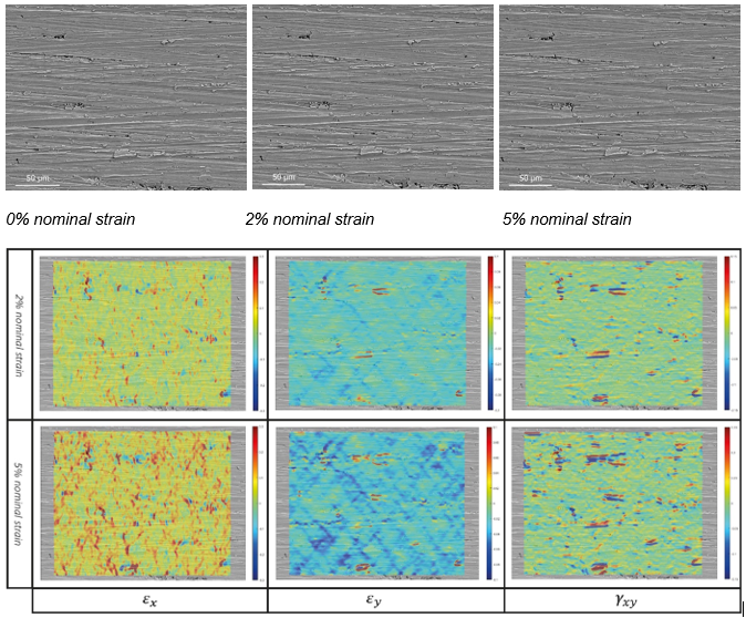
By correlating the high-resolution images of the sample surface before and after its deformation during the in-situ experiment, the local surface strain can be evaluated by means of DIC. A selected area close to the center of the Cu sample is imaged with a high pixel density of 4000 x 3000 pixels at different nominal strain levels using the chamber SE detector. In this selected area, the local normal strain in the x direction is significantly larger than the nominal strain value, and the strain is mainly concentrated around the micrometer sized cracks which grow and propagate during the in-situ experiment (Figure 1).
Further advancements such as automated feature tracking, autofocus and multiple regions of interest (ROIs) help to realize true one-button-start workflows and experiments. Results such as grain boundary transition or grain deformation imaged using backscattered electron detection (BSD) at high temperatures will be shown. Examples of measuring grain misorientation during mechanical loading by means of high-resolution EBSD as well as high resolution strain mapping using DIC will also be discussed.
Fig. 1: Local strain distributions of Cu surface at different elongations during in-situ tensile testing are analyzed by means of digital image correlation (DIC).
- References
[1] ] Open source 2D digital image correlation GOM Correlate, http://www.gom.com