Beam broadening of keV-electrons in matter calculated by numerical solution of the transport equation
- Abstract number
- 297
- Event
- European Microscopy Congress 2020
- DOI
- 10.22443/rms.emc2020.297
- Corresponding Email
- [email protected]
- Session
- PST.3 - New Instrumentation
- Authors
- Dr. Erich Müller (1, 2), M.Sc. Milena Hugenschmidt (1, 2), Prof. Dagmar Gerthsen (1, 2)
- Affiliations
-
1. Laboratory for Electron Microscopy, Karlsruhe Institute of Technology (KIT)
2. 3DMM2O - Cluster of Excellence (EXC-2082/1 – 390761711), Karlsruhe Institute of Technologie (KIT)
- Keywords
beam broadening, electron transport equation, numerical solution
- Abstract text
Electron microscopy at low primary electron energies E0 ≤ 30 keV has experienced increasing interest in the past years. At such low electron energies, the signal-to-noise ratio for material contrast is enhanced and knock-on-damage is reduced compared to higher electron energies. However, at lower energies, the mean free path length decreases, more scattering events take place and the electron beam broadens by plural and multiple scattering in the material even for small sample thicknesses. This leads to a progressive worsening of the lateral resolution with increasing penetration depth.
Several analytical approaches to determine electron beam broadening have been published. Frequently applied is the analytical description of Goldstein et al. [1] based on Rutherford scattering of electrons in matter. Gauvin et al. [2] published an elaborated theory of electron beam broadening. They describe beam broadening b by Eq. (1) and distinguish different scattering regimes by different Hurst exponents H:
H is 0.5 for the diffusion regime and reaches H = 1 close to the ballistic regime while values H < 0.5 stand for subdiffusion scattering. R denotes the percentage of the total beam intensity that defines the beam radius. E0 is the primary electron energy, t the sample thickness, while the density ρ, atomic number Z and atomic mass A accounts for the investigated material. Hugenschmidt et al. [3] experimentally verified Eq. (1) by scanning transmission electron microscopy for different materials and electron energies.
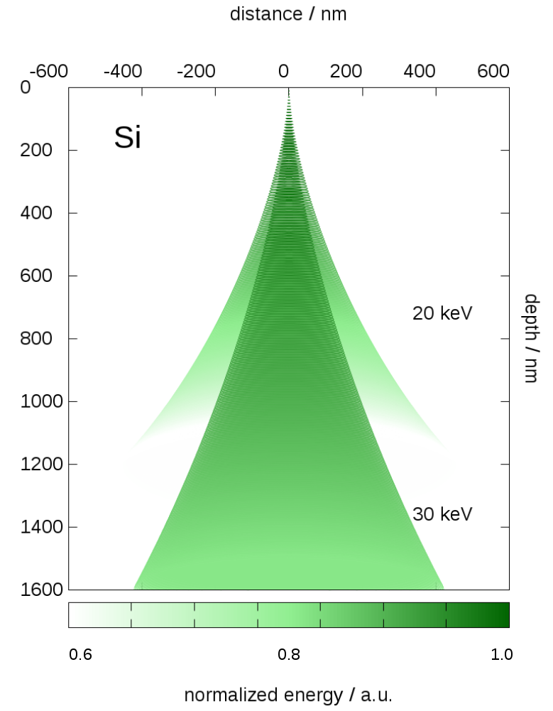
In this work, we focus on the calculation of the electron beam broadening by numerically solving the multiple-scattering algorithm of Goudsmit-Saunderson similar to the description of Negreanu et al. [4]. A number of 500 coefficients in the Legendre expansion were calculated by using the N-point Gauss-Legendre integration formula for different electron energies. Screened Rutherford differential scattering cross-sections were used and energy loss was considered by a continuous slowing down approximation. Our program CeTE provides the angular distribution and energy of the scattered electron after passing a given path length. Following Bielajew et al. [5] the mean penetration depth and lateral displacement of the scattered electrons were calculated from the moments of the probability distribution given by CeTE. Fig. 1 shows the calculated penetration depth and lateral displacement of a 20 keV and 30 keV focused primary electron beam scattered in silicon. The color fading indicates the energy loss of the primary electrons while propagating in the material.
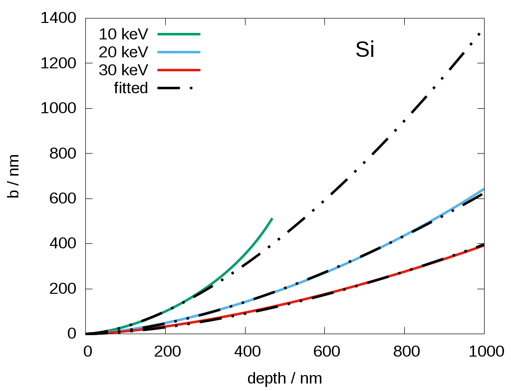
Beam broadening is determined on the basis of data obtained by CeTe from the mean displacement of the electrons after traveling a distinct path length from the sample surface. The mean beam radius is plotted in Fig. 2 by colored lines for different electron energies as a function of the penetration depth in silicon. To compare the CeTE calculations with Eq. (1), R = 0.5 is chosen corresponding to a width of the beam containing 50 % of the electrons. By fitting factor H, the values obtained by Eq. (1) are plotted by dash-dotted lines in Fig. 2. The best match was obtained for H = 0.6 indicating a scattering regime close to diffusion. For thinner samples, the fit yields higher H values, following as expected the trend to predominant forward scattering. When the scattered electrons have lost most of their energy, the lateral displacement increases more pronounced than predicted analytically by Eq. (1) as can be seen in Fig. 2 for 10 keV electrons (green line in Fig. 2). The generalized Eq. (1) does not consider the limit of the scattering regime, where the electrons approach their maximum penetration depths. Nevertheless, the distributions and moments of the numerical solution of the transport equation give insights to the electron scattering at all regimes mentioned here.
Figure 1. Penetration depth and displacement of 20 keV and 30 keV electrons scattered in silicon. A relative colour scale indicates the energy of the electrons after travelling a distinct path length.
Figure 2. Beam broadening in dependence of the mean penetration depth for a beam radius containing 50% of the scattered electrons for different energies (coloured lines) calculated by CeTe. Calculated data on the basis of Eq. (1) are plotted with dashed-dotted lines for a fit parameter H = 0.6.
- References
[1] J Goldstein et al., Scanning Elecron Microscopy 1 (1977), p. 315.
[2] R Gauvin et al., Ultramicroscopy 167 (2016), p. 21.
[3] M Hugenschmidt et al., Journal of microscopy 274 (2019), p. 150.
[4] C Negreanu, Radiation Physics and Chemistry 74 (2005), p. 264.
[5] AF Bielajew et al., Nuclear Instruments and Methods B173 (2001), p. 332.
[6] We acknowledge funding by the Deutsche Forschungsgemeinschaft (DFG, German Research Foundation) under Germany’s Excellence Strategy – 2082/1 – 390761711.