Beam-dose controlled atomic resolution EELS mapping of catalyst supports
- Abstract number
- 757
- Event
- European Microscopy Congress 2020
- DOI
- 10.22443/rms.emc2020.757
- Corresponding Email
- [email protected]
- Session
- PST.4 - Spectroscopies in Electron, X-ray and Ion Microscopy
- Authors
- Trung D. Tran (1), Dogan Ozkaya (1)
- Affiliations
-
1. Johnson Matthey Technology Centre
- Keywords
Atomic resolution, EELS, spectroscopy, STEM
- Abstract text
Probe-corrected STEM leads to not only incoherent and high-resolution imaging of individual atomic columns but also to spectroscopic imaging based on STEM-EELS at atomic level [1]. Also, through developments made in instrumentation [2, 3], extracting signal components from spectrum images using Multivariate Statistic Analysis (MSA) [3] and formulating the physics of delocalisation and radiation damage associated with electron-electron inelastic scattering [4], spectroscopic imaging has become a routine analytical technique. However, many of the practical atomic resolution EELS mapping experiments has been successfully demonstrated on beam-stable (less sensitive to knock-on damage) crystalline structures (usually perovskite-like).
Although being established as a popular and fascinating technique, EELS atomic resolution mapping is still challenging for a range of various crystalline samples including nanoscale ones, mainly due to the stability issue. Tackling this depends on optimisation of detection and balancing between beam dose and signal/noise ratio.
Here we will demonstrate that combination of experimental design and data processing (including MSA-based denoising) is necessary based on a study of signal collection efficiency and sample stability. The advantage of multiple-frame acquisition will also be demonstrated.
Some of the developments (including dual-EELS [5]) has made a significant difference in EELS technology and has produced maps far superior to EDX in most of modern atomic-resolution systems, not only for spatial & energy resolution but also for signal/noise even at high energy loss (above ~2000 eV) excitations.
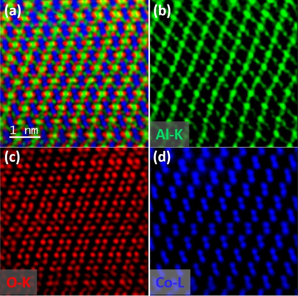
Figure 1 shows EELS mapping of Al (K-edge), O (K-edge) and Co (L-edge) in the [101] zone axis of a cobalt blue (CoAl2O4) [6] crystal.
Figure 1. (a) Superimposed EELS maps of [101] CoAl2O4; (b) Al (green); (c) O (red) and (d) Co (blue)
- References
[1] S J Pennycook et al, J. Electron Microscopy, 58[3] (2009), 87.
[2] O L Krivanek, Microsc. Microanal. Microstruct, 2 (1992), 315.
[3] M Watanabe, M Kanno and E Okunishi, JEOL News, 45 (2010), 1.
[4] R F Egerton, Ultramicroscopy, 180 (2017), 115.
[5] J Scott et al, Ultramicroscopy, 108 (2008), 1586.
[6] The authors would like to thank Dr. Peter Ellis for a standard sample of cobalt blue.