Broad Argon Ion Beam (BIB) Milling to improve EBSD analysis of a nickelbase alloy using a modern Schottky FE-SEM
- Abstract number
- 1327
- Event
- European Microscopy Congress 2020
- DOI
- 10.22443/rms.emc2020.1327
- Corresponding Email
- [email protected]
- Session
- PST.5 - Diffraction techniques and structural analysis
- Authors
- Dr. Roland Schmidt (1)
- Affiliations
-
1. Hitachi High-Technologies Europe GmbH
- Keywords
High speed EBSD, Nickelbase alloy, Broad Ion Beam, Schottky FE-SEM, Kikuchi, ion milling
- Abstract text
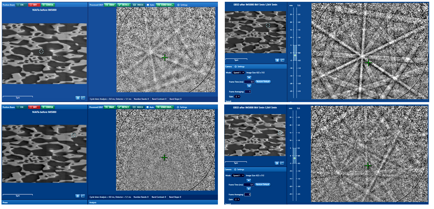
Modern Electron Backscattered Electron Diffraction (EBSD) detectors have the potential to index a Kikuchi pattern, the diffraction pattern of crystalline materials in the SEM, in less than a ms. Supported by an analytical SEM with high probe currents quality EBSD mappings can be recorded within a few minutes. However, often the surface of crystalline materials is not anymore crystalline, because a contamination layer has been adsorbed from exposure to the atmosphere, an amorphous oxid layer has grown or the surface was damaged by the foregoing conventional mechanical preparation procedures.
Broad Ion Beam (BIB) milling is a complementary SEM sample preparation technique which can be used to create nearly artefact free cross sections of complex multi-layers and composite joints, even down to the few nm scale. The quality of BIB cross sections is comparable to those produced in a focused ion beam system, but the milled area is much wider, up to a few mm [1]. The method facilitates to see the electron channeling contrast of crystaline materials similar to a focused ion beam (FIB) image [2],[3]. Additionaly it can be applied to existing embedded cross sections which require a flat polishing finish to remove surface contaminations without damaging the crystal and thereby opens the surface for the EBSD technique. This work describes the effective application of BIB with a Hybrid Ion Milling System IM5000 to the EBSD analysis of a 2-phase as cast nickelbase alloy before and after BIB endpolishing. The measurements were performed with a Hitachi Schottky FE-SEM SU7000 equipped with an Oxford symmetry EBSD detector. Fig.1 shows Kikuchi patterns before ion milling in the NiAl-phase (top left) and the Ni-phase (bottom left) before and after (right) Broad Ion Milling using Ar-ions at 1.5kV. The resulting EBSD mappings using inverse pole figures and phase distributions will be shown. An explanation refers to a similar problem in HR-TEM of crystalline materials, where the Ga-ions of FIB prepared TEM lamellae may destroy the atomic lattice and its visibility.Fig. 1: EBSD spot analysis in a 2-phase Nickelbase alloy before (left) and after Broad Ion Milling (right) using 1.5kV Ar-ions.
- References
[1] Christopher Gort, Charge Carrier Dynamics in Perovskites, masters thesis, Johannes Gutenberg Universität Mainz, 2019
[2] Tomohiro Kato et al, J. Phys.: Conf. Ser.871 012044 (2017) p.1
[3] J. Teshima e.a., microscopy today, Sept (2013) p. 56