Cathodoluminescence and Electron Holography complementary studies of AlN/GaN nanowires
- Abstract number
- 1012
- Event
- European Microscopy Congress 2020
- DOI
- 10.22443/rms.emc2020.1012
- Corresponding Email
- [email protected]
- Session
- PSA.3 - Semiconductors & Devices
- Authors
- Sophie Meuret (1), Luiz Tizei (3), Bruno Daudin (2), Christophe Gatel (1)
- Affiliations
-
1. CEMES/CNRS
2. INAC/CEA
3. Laboratoire de Physique des Solides
- Keywords
III-V semiconductor
Cathodoluminescence
Electron Holography
- Abstract text
III-V semiconductor heterostructures are essential opto-electronic materials (LEDs, solar cell...). Their optical properties are governed by structure well below the light diffraction limit (~300 nm). It is possible to study this structure at the nanoscale in electron microscopy. In particular, cathodoluminescence spectroscopy in a transmission electron microscope can study the emission spectrum of individual quantum wells [1] . However, the excitation mechanism from the electron interaction to the excitation of light is quite complicated and limits the quantitative study of its local optical properties (quantum efficiency, absorption cross section...). III-V nanostructures have an intrinsic electric field along the growth direction of the different layers that induce a redshift of the luminescence as well as a drastic decrease in the efficiency of excitation[2], [3]. This effect is called the quantum Stark effect. The corresponding electric field can be screened by charge carriers created by the optical or electron excitation. Therefore, electron holography, a powerful electron imaging technique that map the electric and magnetic field at the nanoscale, is a perfect complementary technique to study such structure [4].
In this presentation we will discuss the study both with cathodoluminescence and electron holography of the same heterostructure (see Figure 1). We will, especially, investigate the fundamental properties of the charge carriers generated by the electron-matter interaction and discuss the different between TEM and STEM excitation.
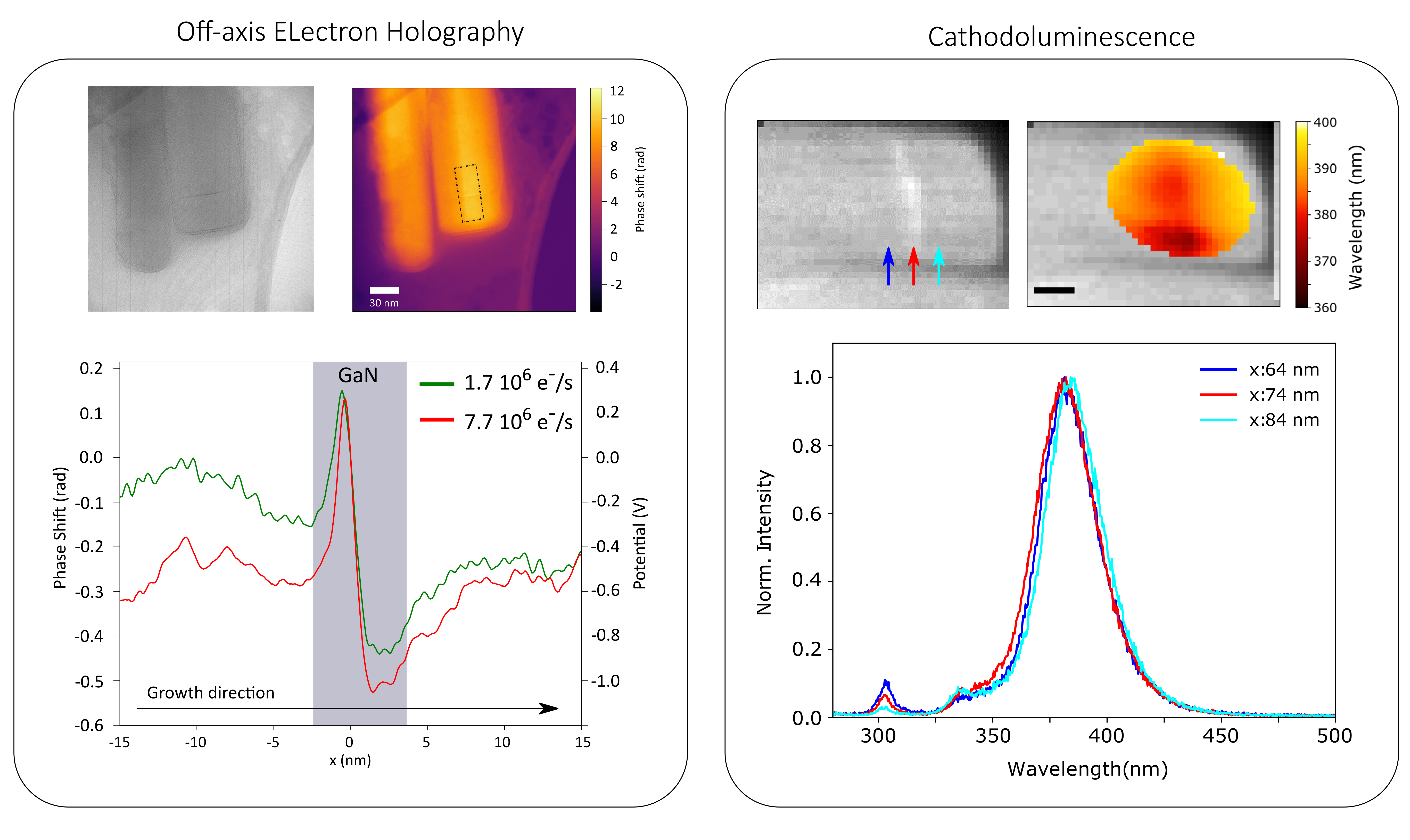
Figure 1 : Electron Holography and cathodoluminescence measurements of the same AlN/GaN nanowire. Electron holography experiment seems to show a screening of the electric field when the electron dose increases (red curve). The cathodoluminescence experiment show a red shift of the luminescence spectrum when the electron excites the material outside of the quantum wells (cyan arrow and spectrum).
- References
[1] L. F. Zagonel et al., “Nanometer scale spectral imaging of quantum emitters in nanowires and its correlation to their atomically resolved structure,” Nano Lett., vol. 11, no. 2, pp. 568–573, 2011.
[2] P. Lefebvre and B. Gayral, “Optical properties of GaN/AlN quantum dots,” C.R. Phys., vol. 9, pp. 816–829, 2008.
[3] L. F. Zagonel et al., “Nanometer-scale monitoring of quantum-confined Stark effect and emission efficiency droop in multiple GaN/AlN quantum disks in nanowires,” Phys. Rev. B, vol. 93, no. 20, pp. 1–12, 2016.
[4] D. Cherns, H. Mokhtari, C. G. Jiao, R. Averbeck, and H. Riechert, “Profiling band structure in GaN devices by electron holography,” J. Cryst. Growth, vol. 230, pp. 410–414, 2001.