Damage-free sample preparation of metallic microwires using an adapted electropolishing method.
- Abstract number
- 406
- Event
- European Microscopy Congress 2020
- DOI
- 10.22443/rms.emc2020.406
- Corresponding Email
- [email protected]
- Session
- PSA.2 - Metals & Alloys
- Authors
- Dr. Saeid Pourbabak (1), Dr. Andrey Orekhov (1), Prof. Dr. Dominique Schryvers (1)
- Affiliations
-
1. University of Antwerp
- Keywords
electropolish, metal, microwire, Ni-Ti
- Abstract text
Very few TEM studies have been performed on metallic samples smaller than the conventional 3 or 2.3 mm discs and prepared by electropolishing. Still, the at present currently used FIB techniques for thinning to electron transparency introduce radiation damage of different kinds, always implying uncertainties on the findings of such investigations. Stickler & Engle [1] electropolished 1 mm diameter wires of tungsten and bismuth telluride in a two–step procedure of indentation and thinning of the center of the wire which is, however, not practical for wires thinner than 1 mm. Kestel [2] introduced three methods in which small sized samples were plated, attached or embedded with a surrounding metal yielding a 3 mm disc. The idea of enlarging the sample to a 3 mm size was retained in the present work, but due to the further reduction of the size of the original material, an alternative approach had to be introduced which does not have the disadvantage of manipulating the specimen at high temperature or contaminating it with other metals, as is unavoidable in the Kestel procedure. The concept of this work is shown using the above-mentioned Ni–Ti microwires, but is applicable to every metallic microwire of similar size when adapting the electrochemical thinning conditions (chemical solution, voltage, temperature, …).
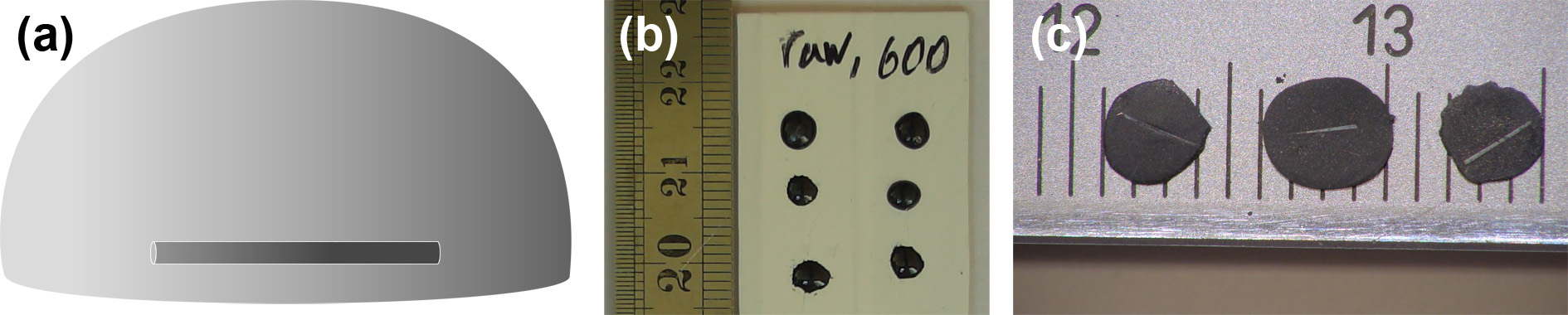
The main idea is to embed the microwire under consideration in a medium in a way that 1) the obtained complex fits into the clamping holder of a twin–jet electropolishing unit, which means having a disc shape of 3 mm diameter and ~150 µm thickness, 2) the wire is exposed on both sides of the embedding disc so that it can be reached by the electrolyte during the process, 3) there is electric contact between the wire and the holder and 4) the medium is non-transparent to light so that the automatic hole detecting system can be employed. In the present case, this was obtained by embedding the wire in an EPO–TEK 353ND epoxy resin with an addition of 10 wt.% graphite powder with particle size of ~5 μm and ensuring that the wire physically touches the anode of the holder. Such samples are produced by chopping the wire into pieces of ~2 mm and placing these on a microscope glass slide wrapped in Teflon tape which eases detaching the resin after hardening. A drop of resin mixture was placed on each wire piece using a needle. The resin drop should be big enough to make a hemisphere with a diameter of appr. 3 mm, completely covering the wire, as schematically shown in Figure 1(a). Due to the still viscous nature of the resin some resin will flow underneath the wire, but most of the resin will form the hemisphere above the wire. The resin was then left to harden at room temperature which took about 4 days. An image of hardened hemisphere resins is shown in Figure 1(b). Then each disc is mechanopolished from both sides until a thickness -of ~100 µm was obtained with the wire surface appearing from both sides of the disc (Figure 1(c)). The current Ni-Ti microwires under investigation are in the B2 phase at room temperature and do not contain any full–grown precipitates and thus the mixture of 20% sulfuric acid in 80% methanol operating at 18 V (0.13 A) and 0 °C was used.
Figure 1 (a) Schematic of the wire embedded into a hemisphere resin, (b) hardened hemisphere resin containing wires, (c) mechanopolished discs.
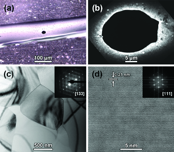
In Figure 2(a), a light optical microscope (LOM) image of a Ni-Ti microwire TEM specimen obtained by the above method is shown. In this image the perforation in the center of the wire is clearly seen. The corresponding low magnification scanning TEM (LM–STEM) image is shown in Figure 2(b) revealing good thinning around the entire hole. A higher magnification bright field (BF) TEM image is presented in Figure 2(c) together with a selected area electron diffraction pattern (SAED) as inset. Figure 2(d) a high resolution (HR)–STEM image along the 〈111〉B2 direction is presented. The BF TEM image, the diffraction pattern as well as the HR–STEM showing atomic resolution clearly indicate the local quality of the thinning procedure. The grains in Figure 2(c) do not contain any thinning induced defects, the thickness allows for the observation of diffuse intensity in the SAED inset and referring to local ordering [3] and the high resolution in Figure 2(d) reveals a perfect lattice without precipitation.
Figure 2 (a) LOM image of the specimen after electropolishing showing the perforation in the wire, (b) LM–STEM image of the specimen shown in a, (c) a BF–TEM image of some grains of the wire together with the SAED pattern (inset), (d) HR–STEM image with the corresponding fast Fourier transformation (inset).
- References
[1] R Stickler and RJ Engle, Journal of Scientific Instruments 40 (1963), p. 518.
[2] BJ Kestel, MRS Online Proceedings Library Archive, (1990) Vol. 199.
[3] S Pourbabak, X Wang, D Van Dyck, B Verlinden and D Schryvers, Functional Materials Letters 10 (2017), p. 1740005.