Deconvolving multi-phase SPED datasets: Machine learning assisted pattern matching for phase determination in thin film based oxide electronic devices
- Abstract number
- 1364
- Event
- European Microscopy Congress 2020
- DOI
- 10.22443/rms.emc2020.1364
- Corresponding Email
- [email protected]
- Session
- PST.5 - Diffraction techniques and structural analysis
- Authors
- Alexander Zintler (2), Robert Eilhardt (2), Dr. Shuai Wang (2), Dr. Matus Krajnak (1), Patrick Schramowski (2), Wolfgang Stammer (2), Dr. Stefan Petzold (2), Kaiser Nico (2), Prof. Kristian Kersting (2), Prof. Lambert Alff (2), Prof. Leopoldo Molina-Luna (2)
- Affiliations
-
1. Quantum Detectors
2. Technical University of Darmstadt
- Keywords
machine learning, precession electron diffraction, resistive memory
- Abstract text
Scanning precession electron diffraction (SPED) datasets containing single diffraction patterns which include information from more than a single phase can be deconvolved by using machine learning algorithms. In this work we use blind source separation routines to extract components from a dataset of a planview prepared thin film stack. Local epitaxial conditions can be extracted in direct correlation between different layers in the stack.
Improving device reliability and performance in oxide electronic-based resistive memory applications requires a profound understanding of the microstructure and atomistic processes which define the device properties. Here, we investigated a molecular beam epitaxy (MBE) grown thin film stack which exhibits a highly textured growth due to the epitaxial growth conditions in the molecular beam epitaxy (MBE) deposition process [1]. The grain boundaries present in this system have a strong influence on the macroscopic device behavior due to their inherent physical properties, i.e. localized high defect concentration [2] and increased vacancy mobility [3].
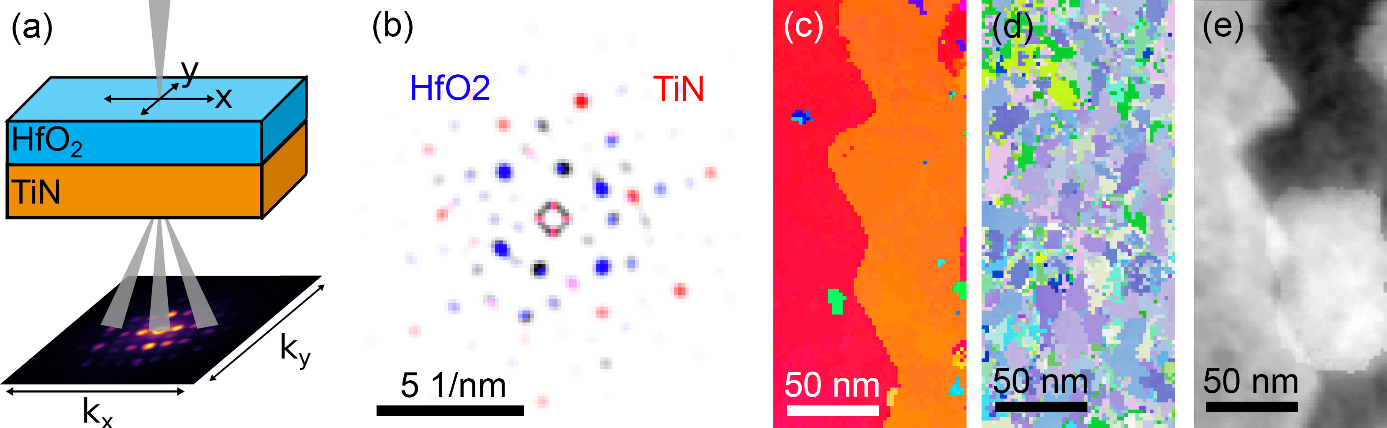
While 4D-STEM methodologies can resolve the relevant structural features [4], acquiring statistical information is a time-consuming process. Here, we present a procedure that allows for fast acquisition of spatially correlated, multi-phase information in a two (or more) layered thin film stack. By transmitting a precessing quasi-parallel STEM beam through the sample (see Figure 1(a)) a four-dimensional data set is generated. In our setup, an NBD probe (in 2D real space) is scanned over the sample and reciprocal space information is collected on a fast pixelated single electron detector (MerlinEM, Quantum Detectors).
The stack was FIB prepared in plan-view geometry which allows the direct correlation of the epitaxial texture transfer for each individual HfO2 grain over a large sample area. The result is a set of superimposed diffraction patterns of all sampled phases contained in the stack (see Figure 1(b)). In order to distinguish between phases, we applied both, pattern matching (PM) and machine learning (ML) based blind source separation (BSS) routines [5]. Conventional PM yields a low reliability phase recognition for a mixed/superimposed diffraction pattern. Using a list of components generated by unsupervised singular value decomposition (SVD), the raw data were filtered. This yields an improved PM result. Recent developments in ML mainly contributed to the advancements in deep learning, have brought large improvements to interdisciplinary fields, e.g. signal processing and microscopy [6]. Deep neural networks (DNN) therefore present a promising extension to the ML based BSS routines. Deconvolving multi-phase superimposed SPED datasets, as presented here, can offer a unique and statistical way of analyzing complex crystalline thin film stacks with a high spatial resolution.
Figure 1: (a) Quasi-parallel 4D-STEM (SPED) and plan-view sample geometry, (b) single color-coded superimposed diffraction pattern of a HfO2 (blue) and a TiN grain (red), (c) orientation map (IPF color-coding) of the TiN phase and (d) of the HfO2 phase for the same area, (e) exemplary extracted SVD loading revealing one of the TiN grain orientations. The component also reveals amorphous carbon contamination.
- References
[1] Petzold S et al., Adv. Electron. Mater. 10 (2019)
[2] Xue K-H et al., Appl. Phys. Lett. 20 (2013)
[3] McKenna K et al., Appl. Phys. Lett. 22 (2009)
[4] Ophus C, Microsc. Microanal. 3 (2019)
[5] Duncan N. Johnstone et al., pyXem 0.10.1 (2020)
[6] Borodinov N et al., Npj Comput. Mater. 1 (2019)
[7] The authors acknowledge financial support from the Deutsche Forschungsgemeinschaft (DFG) under research grant MO 3010/3-1 and the European Research Council (ERC) “Horizon 2020” Program under Grant No. 805359-FOXON.