Electric Field-Induced Surface Melting of Gold at Room Temperature visualized at Atomic Resolution Using In Situ TEM
- Abstract number
- 1421
- Event
- European Microscopy Congress 2020
- DOI
- 10.22443/rms.emc2020.1421
- Corresponding Email
- [email protected]
- Session
- PST.6 - In-situ and in-operando microscopy
- Authors
- Ludvig de Knoop (1), Mikael Juhani Kuisma (3), Joakim Löfgren (1), Kristof Lodewijks (1), Mattias Thuvander (1), Paul Erhart (1), Alexandre Dmitriev (2), Eva Olsson (1)
- Affiliations
-
1. Chalmers University of Technology
2. University of Gothenburg
3. University of Jyväskylä
- Keywords
In situ TEM biasing, ab initio molecular dynamics simulations, surface disorder, field evaporation
- Abstract text
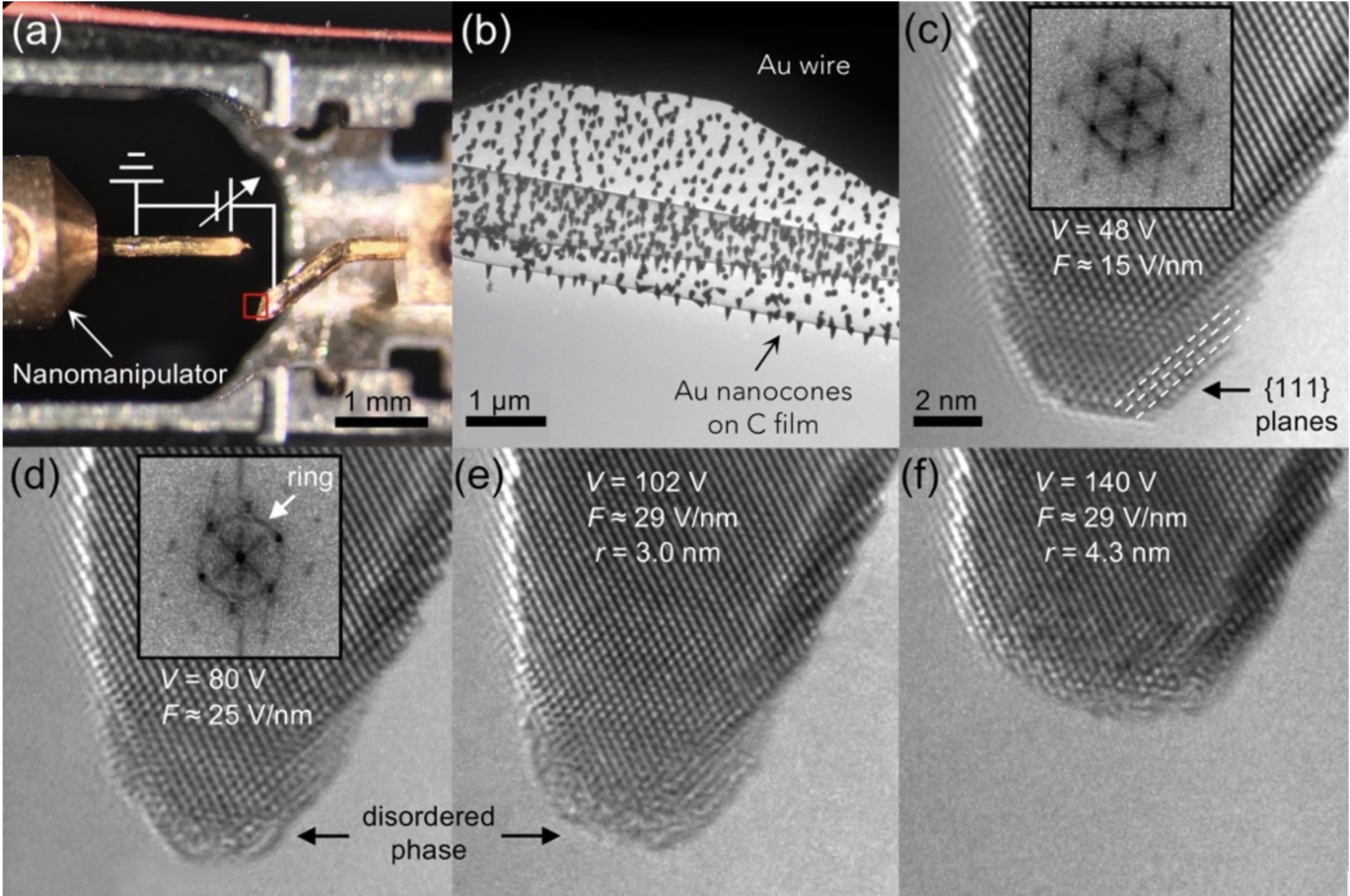
Induced by an electric field of the order of 25 V/nm, we have melted the surface of gold (Au) nanocones using in situ transmission electron microscopy (TEM). The melted surface was observed as a structural disorder in the outmost 2-4 atomic layers [Figs. 1(d) and 1(e)]. Ab initio molecular dynamics simulations confirm the experimental results.
As is well known, elevating the temperature of metals can induce surface melting and surface roughening [1]. Not only elevated temperatures, but also intense electric fields can change the surface structure, e.g. in field evaporation utilized in atom probe tomography. However, as far as we know, no atomically resolved observations of a metal surface at electric fields just below the field-evaporation field exists.
Here, we have imaged the surface of Au nanocones while simultaneously applying an intense electric field using a Nanofactory Instruments in situ TEM biasing and nanomanipulation system. At field strengths of around 25 V/nm, the surface altered from crystalline [Fig. 1(c)] to disordered, or, surface melted [Figs. 1(d) and 1(e)]. When reducing the electric field, the disordered layers reverted back to the ordered crystalline structure showing that the process is reversible. The insets in Figs. 1(c) and 1(d) display fast Fourier transformations (FFTs) of the apex of the Au nanocone before and after the phase transformation, respectively. The FFT in Fig. 1(c) is typical for a crystalline structure, whereas the ring observed in the FFT in Fig. 1(d), is indicative of the observed disordered or surface melted state. When we increased the electric field even further, to around 30 V/nm, the atoms field evaporated, which can be observed in Fig. 1(f) as a shortening of the Au nanocone.
To understand the mechanisms behind the observed phenomenon, extensive ab initio molecular dynamics simulations were made. At electric fields of 25 V/nm, the simulations show an increased atom mean square displacement corresponding to a temperature increase of around 50 K. This is not sufficient to explain the observed disordered or surface melted state but the simulations also reveal that the surface melted state could be attributed to a vanishing energy cost for the formation of surface defects at high electric fields.
To be able to reversibly switch a metal surface structure on the atomic level, using an electric field, can enable new applications in catalysis and field-effect technology, as well as open up new research fields in e.g. low-dimensional phases of matter.
Figure 1. (a) The nanomanipulator and sample with electrical circuit schematic overlay in the front part of the in situ TEM sample holder. (b) TEM micrograph of the Au nanocones on a carbon film. The micrograph is part of the area indicated by the red square in (a). (c)-(f) show TEM micrographs of the apex of the Au nanocone before (c) and after (d)-(f) the phase transformation. In (c), with an applied voltage V = 48 V resulting in an electric field F ≈ 15 V/nm, the nanocone is crystalline. In (d), at F ≈ 25 V/nm, the outmost atomic layers have switched to a disordered or surface melted phase, indicated also by a ring in the fast Fourier transformation inset. Increasing the electric field further, the atoms start to evaporate in (e), which is clearly seen as a shortening of the nanocone in (f). The scale bar in (c) applies also to (d)-(f).
- References
[1] J. W. M. Frenken and J. F. van der Veen, Phys. Rev. Lett. 54 (1985), p. 134.
[2] L de Knoop et al., Physical Review Materials 2 (2018), p. 085006.