Electron Interference Experiment by using V-Shaped Double Slit
- Abstract number
- 136
- Event
- European Microscopy Congress 2020
- DOI
- 10.22443/rms.emc2020.136
- Corresponding Email
- [email protected]
- Session
- PST.2 - Microscopy for the study of quantum effects and nano-optics
- Authors
- Dr Ken Harada (4), Dr Yoshio Takahashi (1), Dr Tetsuya Akashi (1), Dr Yoshimasa Ono (4), Prof Tetsuji Kodama (2), Prof Shigeo Mori (3)
- Affiliations
-
1. Hitachi, Ltd.
2. Meijo University
3. Osaka Prefecture
4. RIKEN
- Keywords
electron interferometry, double slit, interference experiment, wave/particle duality, quantum physics
- Abstract text
Young’s double-slit experiment is one of the world-famous experiments to visualize the mystery of quantum physics, wave/particle duality of electrons. We have been conducting the double-slit experiments to clarify which slit electrons passed through by using asymmetric double slits [1]. As a result, we noticed that two waves passed through the right and left slits always overlapped because of the existence of a defocusing distance due to a propagation distance from the slit opening to the recording plane. To overcome this difficulty, we developed an optical system for imaging a double slit placed on the observation plane under the infocus condition [2] by using two electron biprisms [3] for superimposing two waves from each slit opening. The double slit was V-shaped made of about 1.3-mm-thick Cu foil manufactured by using a focused ion beam instrument [2]. For interference experiment we used a 1.2-MV field-emission electron microscope having excellent coherence [4].
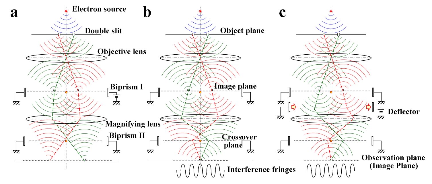
Figure 1 shows a schematic diagrams of the optical system for this study; (a) non-interference condition without bias voltage to the biprism II, (b) interference condition with bias voltage to the biprism II (with a phase shift j = 0), and (c) phase-shifted condition using a deflector (j = p). The V-shaped double slit was placed on the object plane. The biprism I was placed on the image plane of the objective lens, the biprism II was placed on the crossover plane under the magnifying lens, and the deflector was placed on an image plane under the double slit. Interference conditions on the observation plane were controlled by the applied voltage to the biprism II and phase shifts between the electron waves were realized by using the deflector.
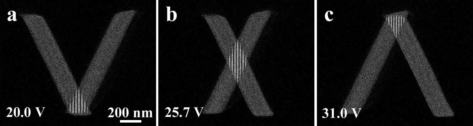
Figure 2 shows interference images of the V-shaped double slit controlled by bias voltages to biprism II; (a) 20.0 V, (b) 25.7 V, and (c) 31.0 V. When no information existed regarding which slit electrons passed through, interference fringes were obtained. To clarify how single electrons build up interference fringes when we do not have appropriate information on which slit electrons passed through, we applied phase shifts between two electron waves by tilting the propagation direction under the double slit.
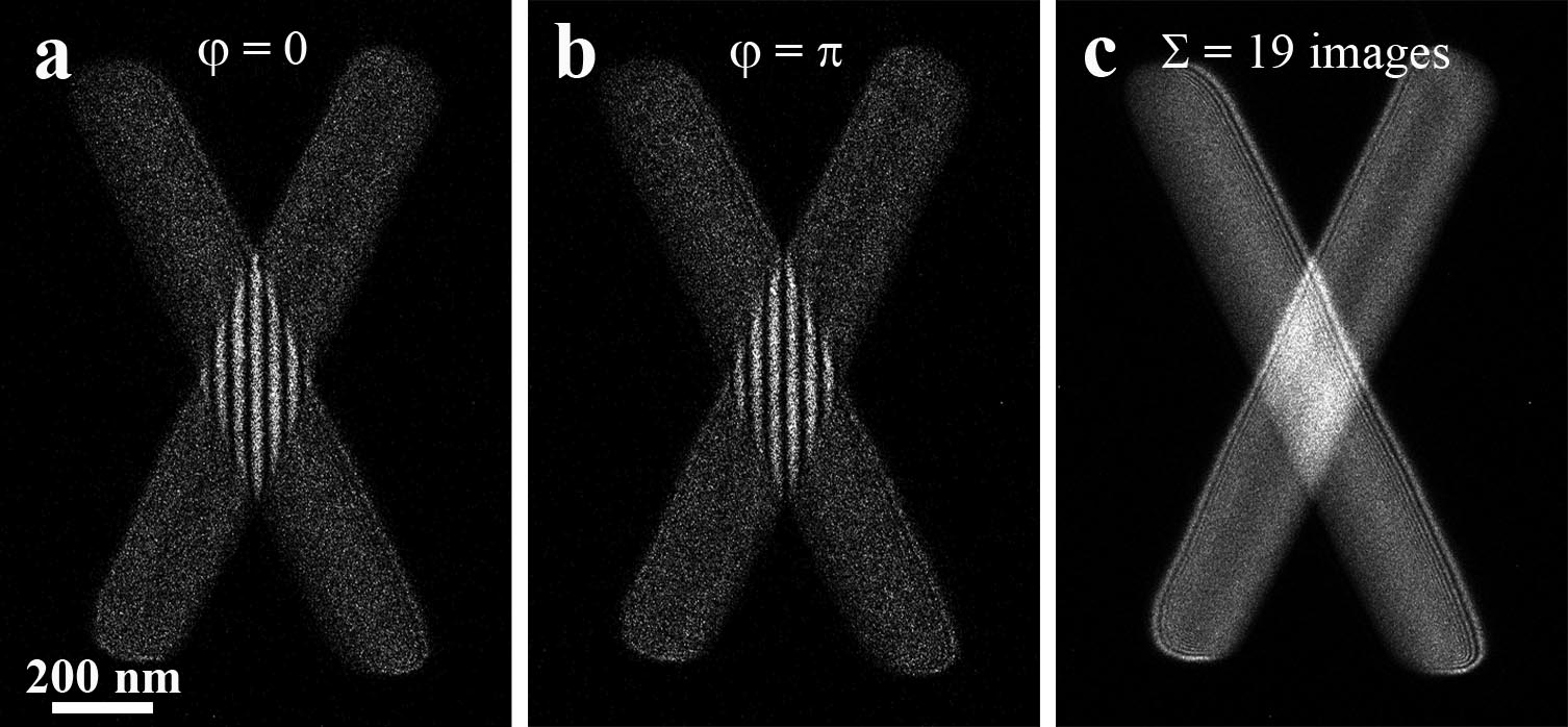
Figure 3 shows interferograms with a relative phase shift j; (a) j = 0, (b) j = p, and (c) integrated image from 19 interferograms for one cycle of the phase shifts. Interferograms in Figs. 3 (a) and (b) have interference fringes composed of electron single-dot images, and interference fringes disappeared almost completely in the integrated image shown in Fig. 3(c). This is not because electron waves have become incoherent.
In conclusion, we developed an optical system for an optically-zero propagation distance. Using a V-shaped double-slit, we succeeded in obtaining interference fringes in the overlapped region and uniform intensity distributions in other regions. Controlling the mutual phase between the two electron waves, we observed that interference fringes changed only their phase positions. Furthermore, interference fringes disappeared in the integrated images composed of single electron accumulation. From these results, relationship between the recording exposure time and beam coherence of electron waves will be examined in future. [5]
Figure 1. Schematic diagrams of the optical system with electron wave propagation profiles: (a) non-interference condition without bias voltage to the biprism II, (b) interference condition with applied voltage (without a phase shift j = 0), and (c) phase-shifted condition using a deflector (j = p).
Figure 2. Series of interference patterns of the V-shaped double-slit with different voltages applied to the biprism II; (a) 20.0 V, (b) 25.7 V, and (c) 31.0 V. Interference fringes were observed only at the two-wave overlapped region, and uniform intensity distributions were observed in other regions.
Figure 3. Interferograms by V-shaped double-slit with a relative phase shift j, (a) j = 0, (b) j = p, and (c) integrated image from 19 interferograms for one cycle of the phase shifts.
- References
[1] K. Harada et al, Scientific Reports, 8 (2018) 1008.
[2] K. Harada et al, Microsc. Microanal., 25 (2019) 944.
[3] K. Harada et al, Appl. Phys. Lett., 84 (2004) 3229.
[4] T. Akashi et al., Microscopy, 67 (2018) 286.
[5] The authors would like to thank Ms. K. Shimada of RIKEN for preparing V-shaped gratings. This work was supported by KAKENHI, Grant-in-Aid for Scientific Research ((B) 18H03475).