Exploring the atomic structure of pyramidal quantum dots
- Abstract number
- 1406
- Event
- European Microscopy Congress 2020
- DOI
- 10.22443/rms.emc2020.1406
- Corresponding Email
- [email protected]
- Session
- PSA.3 - Semiconductors & Devices
- Authors
- Kristina Holsgrove (1), Simone Varo (3), Stefano Moroni (3), Gediminis Juska (3), Demie Kepaptsoglou (2), Quentin Ramasse (2), Ricardo Puebla (1), Hannah McAleese (1), Mauro Paternostro (1), Emanuele Pelucchi (3), Miryam Arredondo (1)
- Affiliations
-
1. Queen's University Belfast
2. SuperSTEM Laboratory
3. Tyndall National Institute, University College Cork
- Keywords
Band-gap, HRSTEM, Pyramids, Quantum, Semiconductors
- Abstract text
Semiconductor quantum dots (QDs) have become a focal point for making quantum information technology a reality, with an endeavour to develop platforms that exceed classical computation and communication. A huge challenge to overcome is achieving large arrays of site-controlled reproducible entangled photon generators which can be integrated into photonic circuits – to date, a difficult requirement to realise. Semiconductor QDs are ideal candidates as they allow photons to be generated on demand, however, existing QD systems are limited by a lack of symmetry, allowing only a small number (1/100 or worse) of effective QDs per photonic chip. Here, a novel pyramidal QD system is presented, which is capable of delivering arrays of highly symmetric and uniform QDs, resulting in an exceptionally high density of entangled-photon emitters [1, 2]. These QDs are fabricated by metal-organic vapour-phase epitaxy (MOVPE) growth inside pyramidal recesses that are lithographically patterned on a (111)B GaAs substrate. The pyramids consist of differently composed III-V (Al)GaAs and InGaAs layers. The GaAs substrate can be removed by back-etching to orient the pyramidal structures in an upright position which enhances the photoluminescence extraction efficiency [3], see Figure 1. Moreover, this system allows the precise stacking of two or more highly symmetric QDs, further allowing the ability to tune the final optical properties [4].
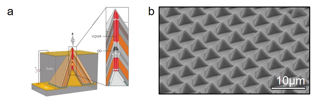
Figure 1. Pyramidal QDs. (a) Schematic of a µLED. The magnified region shows the central part of a pyramid. The epitaxial layers comprise dominant AlGaAs alloys that form a vertical quantum wire (VQWR). Arrows indicate the injection of current. (b) SEM overview of highly symmetrical pyramids after GaAs substrate removal.
Until now, the QD dimensions and crystallographic structure of this high-performing system have been somewhat inferred by scanning electron microscopy (SEM) and atomic force microscopy (AFM) [1]. In this study, we present an extensive characterisation at the micro and nanoscale of this multifaceted and multi-layered 3D pyramidal structure, focusing on locating the source of the entangled photons. Additionally, we report on the challenges that characterising such a complex structure brings. High-end electron microscopy techniques such as high-resolution scanning transmission electron microscopy (HRSTEM) combined with energy dispersive x-ray spectroscopy (EDX) and electron energy loss spectroscopy (EELS) were used to map the chemical composition, see example in Figure 2. We explore the advantages of various specimen preparation techniques and present a novel “lamella flipping” method for low-energy milling of unique pyramidal cross-sections, developed by us to gain a greater insight into the strain distribution and faceted nature of the pyramidal QDs. Furthermore, we investigated local band-gap variations using low-loss EELS at 60kV using a Nion UlstraSTEM 100MC ‘HERMES’ demonstrating a variation of up to ~0.5eV between the GaAs and AlGaAs outer pyramidal layers. We present the extreme difficulties in locating small quantities of indium in 3D structures, discussing effects such as chemical diffusion and correlation to photoluminescence measurements.
We hope to inspire a deeper discussion within the semiconductor community to improve the correlation between the emitters’ positions, faceting effects and crystallographic changes such as impurities or point defects at the atomic-scale [5].
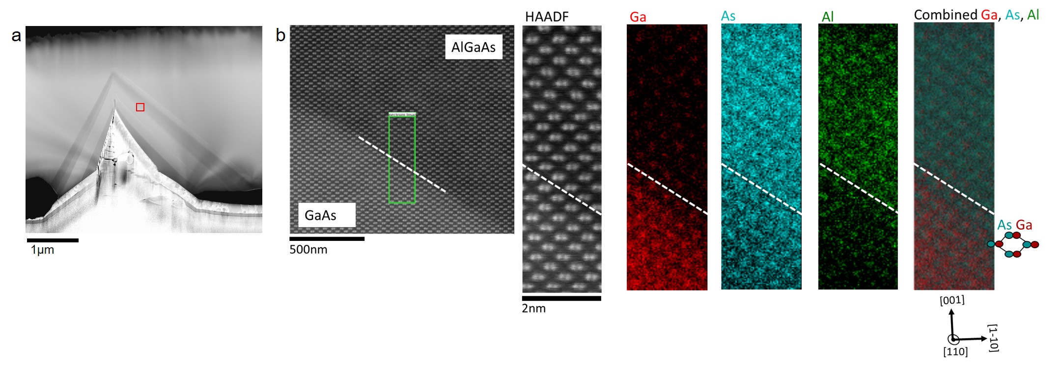
Figure 2. Chemical composition of lll-V layers within a representative pyramid revealed via STEM-HAADF and High-Loss EELS. (a) STEM overview of a cross-section through the centre of a pyramid. (b) Higher magnitude HAADF images and elemental maps. Schematics of the GaAs dumbbells are shown, viewed along the [110] zone axis.
- References
[1] G. Juska, et al., Nature Photonics. 2013, 7 (7), 527-531.
[2] T. H. Chung, et al., Nature Photonics. 2016, 10 (12), 782.
[3] G. Juska, et al., J. Appl. Phys. 2015, 117 (13), 134302.
[4] S. T. Moroni, et al., Appl. Phys. Lett. 2017, 111 (8), 083103.[5] The authors grately acknowledge funding support from SFI-DfE US Ireland 15/1A/2864 and SuperSTEM, the U.K.’s National Facility for Aberration Corrected STEM, funded by the EPSRC.