Gas inclusions within a 5 nm amorphous Al2O3 thin film part of a Memristive Device.
- Abstract number
- 710
- Event
- European Microscopy Congress 2020
- DOI
- 10.22443/rms.emc2020.710
- Corresponding Email
- [email protected]
- Session
- PSA.3 - Semiconductors & Devices
- Authors
- Ole Gronenberg (2), Finn Zahari (1), Dr. Julian Strobel (2), Dr. Georg Haberfehlner (3), Prof. Dr. Gerald Kothleitner (3), Prof. Dr. Lorenz Kienle (2)
- Affiliations
-
1. Institute for Electrical Engineering and Information Technology, Kiel University
2. Institute for Materials Science, Kiel University
3. Institute of Electron Microscopy and Nanoanalysis, Graz University of Technology
- Keywords
EELS, Gas-inclusions, Memristor
- Abstract text
We report the presence of gas (Ar and O2) inclusions inside a 5 nm thin film of amorphous Al2O3, part of a memristive device. Surprisingly, they seem to have no influence on the functionality of the device and they appear in samples prepared by three different oxidation methods. The pore formation mechanism is discussed which is most likely stress evolution during the oxidation of the Al thin film.
Double barrier memristive devices are under investigation, which consist of a 2.5 nm thick NbOx (or HfOx) layer sandwiched between an Al2O3 tunnel barrier and a Schottky-like contact to an Au top electrode. These devices show bipolar interface-based analogue resistive switching which is most probably due to the migration of oxygen vacancies that change the interfacial properties [1]. Inside the tunnel barrier, argon and oxygen gas was found in pores of FIB lamellas which are vacuum-tightly encapsulated in the thin film. The formation and the influence of these pores on the devices are analyzed in this study.
Most probably, Ar stems from the sputtering process and O2 from the oxidation step. Under investigation is the origin of the pores and the influence on the functionality of the memristive devices.
Scanning transmission electron microscopy (STEM) investigations were performed on a monochromated and spherical aberration probe-corrected FEI Titan3 60–300 operated at an acceleration voltage of 300 kV and an approximate dose rate of 106 e nm–2s–1. The STEM is equipped with a GIF Quantum spectrometer for electron energy-loss spectroscopy (EELS). Samples were prepared by focused ion beam milling (FIB) in a dual-beam FIB/SEM instrument and refined by low-energy argon ion polishing in a Fischione Model 1040 NanoMill® system.
Different oxidation methods for the two oxide thin films were tested, including reactive sputtering of NbOx on top of metallic aluminum, thermal oxidation of metallic aluminum at room temperature in oxygen atmosphere in combination with anodic oxidation of metallic Nb as well as thermal oxidation of both metallic layers. Only the first deposition process leads to functional devices. It is assumed that no pores exist in the unoxidized Al thin film because of its good wetting properties on the Nb-back-electrode. Accordingly, an ex situ oxidation of a FIB lamella is planned to gain a better understanding of the pore formation. Additional, functional and non-functional devices from one and the same wafer were investigated with respect to the pores. For this purpose, FIB lamellas were prepared for STEM EELS and EDX analysis and atom probe tomography is scheduled for 3D morphological information of this system.
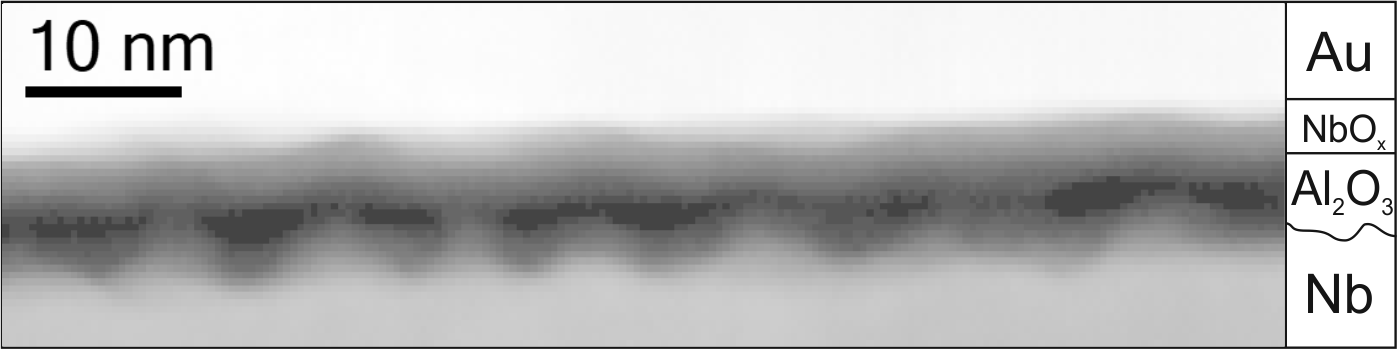
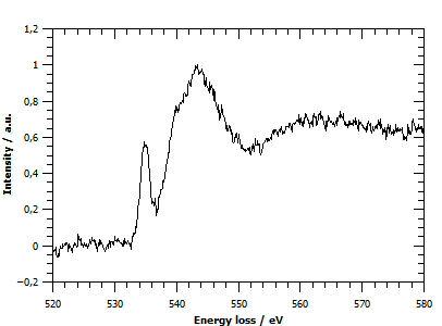
In HAADF STEM images dark contrast is observed in the middle of the Al2O3 thin film indicating pores of approximately 10 nm length and 2 nm thickness (cf. Figure 1). At the same position an oxygen pre-edge peak appears (cf. Figure 2) and further, an Ar-EDX-signal was found at the very same position (approximately 5 at. %). The pre-edge feature most likely originates from the unoccupied π* orbitals of molecular oxygen (gas) [2]. These are strong indications for gas filled pores inside the Al2O3 thin film. Noteworthy, these pores are vacuum-tight in the cross-sectional FIB lamella.
Figure 1: STEM image of the thin film stack with gamma correction to improve the visibility of the pores (dark contrast).
Figure 2: Background subtracted and normalized oxygen K peak with pre-edge feature at 534 eV from the middle of the Al2O3 thin film
Independent of the oxidation method gas filled pores are found inside the Al2O3 thin film after reactive sputtering, anodic and thermal oxidation of the top Nb layer. Accordingly, the oxidation itself is responsible for the pore formation as the metallic Al thin film is assumed to be crystalline and homogeneously deposited on the Nb-back-electrode. It is assumed that the pore formation is based on two triggers. The first is the columnar structure of the Nb thin film. And the second is the expansion during the exothermic oxidation and the following shrinkage during cooling down. Both produces stress in the Al2O3 thin film which may lead to the pore formation. Functional and non-functional devices (checked before FIB preparation) exhibit gas filled pores inside the Al2O3 thin film. Both gas species should behave like ideal dielectrics within an electric field and the pores should be short circuited as they occur in most cases in the valleys of the columnar Nb-back-electrode. Accordingly, it seems convincing that the functionality is independent from the presence of the pores.
Within the tunnel barrier – an amorphous Al2O3 thin film of maximum 5 nm thickness – of a double barrier memristive device planar pores filled with Ar and O2 gas were observed. The formation mechanism is discussed and it is assumed that they form during the oxidation due to stress [3].
- References
[1] M. Hansen et al, Sci. Rep. 5 (2015)
[2] S. Fritz et al, Sci Rep, Bd. 8, Nr. 1, S. 7956, Dez. 2018.
[3] The authors gratefully acknowledge financial support provided by the Deutsche Forschungsgemeinschaft (DFG) in the frame of Research Unit RU 2093 “Memristive Devices for Neural Systems.” This project has received funding from the European Union’s Horizon 2020 research and innovation program under Grant Agreement No. 823717—ESTEEM3.