Growth Dynamics of vertical MoS2 from 3D Focus Ion Beam Tomography
- Abstract number
- 1079
- Event
- European Microscopy Congress 2020
- DOI
- 10.22443/rms.emc2020.1079
- Corresponding Email
- [email protected]
- Session
- PSA.1 - 1D & 2D Materials
- Authors
- Maarten Bolhuis (1), Triantafyllia Sermpeniadi (1), Sabrya van Heijst (1), Sonia Conesa-Boj (1)
- Affiliations
-
1. Delft University of Technology, Kavli Institute of Nanoscience
- Keywords
Energy-dispersive X-ray Spectroscopy (EDX),
Focus Ion Beam Tomography,
High-resolution Transmission Electron Microscopy (HRTEM),
Nonlinear Optics,
Transition Metal Dichalcogenides,
Vertical Molybdenum Disulfide.
- Abstract text
Summary
Transition metal dichalcogenides, such as MoS2, represent promising candidates for building blocks of ultra-thin nanophotonic devices. For such applications, vertically oriented MoS2 (v-MoS2) nanosheets could be advantageous as compared to conventional horizontal MoS2 (h-MoS2) given that their inherent broken symmetry would favor an enhanced nonlinear response. However, the current lack of a controllable and reproducible fabrication strategy for v-MoS2 limits the exploration of this potential. Here we present a systematic electron microscopy characterization of the growth dynamics of v-MoS2 nanosheets based on the sulfurization of a pre-deposited Mo-metal seed layer. We demonstrate the crucial role played by the Mo-metal morphology in determining the resultant growth orientation of the MoS2 nanosheets by means of the combination of 3D focused ion beam (FIB) tomography and transmission electron microscopy (TEM). Our results represent a stepping stone towards the fabrication of low-dimensional TMD-based nanostructures for versatile nonlinear nanophotonic devices.
Introduction
Two-Dimensional (2D) materials such as transition metal dichalcogenides (TMDs) exhibit interesting electronic and optical properties due to their broken inversion symmetry [1]–[3]. Recently a lot of attention has been devoted to the non-linear optical response of these 2D materials [4], [5]. For instance, an enhanced second-harmonic generation has been reported at the edges of horizontal MoS2 (h-MoS2), where the translation symmetry is broken[6]. These findings suggest that vertical MoS2 (v-MoS2), a configuration that maximizes the number of exposed edges, will prove to be more efficient in the context of non-linear nanophotonics devices. Significant progress has been reported on the synthesis of h-MoS2 [7]–[12]. Unfortunately, less is known about the synthesis of v-MoS2. The synthesis of v-MoS2 nanosheets, out of pre-deposited molybdenum (Mo) metal layers, has been achieved by using low reaction temperatures[13]. A different approach is to increase the initial thickness of the pre-deposited Mo-metal layer[14]. Here we show the role played by the Mo-metal morphology in the resulting vertical orientation of the MoS2 nanosheets by combining two complementary techniques, 3-dimensional (3D) focused ion beam (FIB) tomography and transmission electron microscopy (TEM).
Results & Discussion
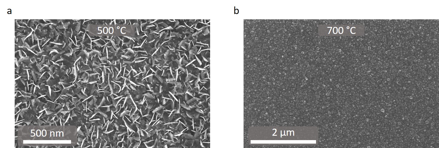
Here a two-step process for synthesizing the v-MoS2 nanosheets has been adopted. Thick Mo‑metal layers of 700 nm were sulfurized at different temperatures in the range between 500 °C and 700 °C [15]. Figures 1a and 1b display top-view scanning electron microscope (SEM) images corresponding to the samples grown at 500 and 700 °C respectively. Whereas the vertical orientation of the MoS2 nanosheets grown at 500 °C can easily be inferred from the SEM image, the orientation of the MoS2 nanosheets grown at 700 °C is more ambiguous. Nevertheless, further investigation with Raman spectroscopy confirmed the presence of v-MoS2 in both samples [15].
Figure 1 (a) and (b) Top view SEM images of samples synthesized at 500 °C and 700 °C.
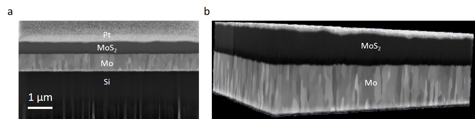
From a single FIB cross-sectional slice used for the 3D reconstruction (Figure 2a), we can identify the MoS2 layer sandwiched in between the protective platinum (Pt) layer and the Mo-metal layer. This cross-section highlights the vertical grains in the Mo-metal prior to sulfurization, arising as a consequence of the magnetron deposition method [16], [17]. Figure 2b displays the complete 3D FIB tomographic reconstruction from the combination of multiple cross-section slices [18]. This reconstruction indicates that the sulfurization of the Mo-metal propagates homogenously through the sample from the top surface downwards to the silicon (Si) substrate.
Figure 2 3D FIB tomography images of the MoS2 and Mo-metal layers. (a) Single cross-section slice. (b) A complete reconstruction of the 3D volume.
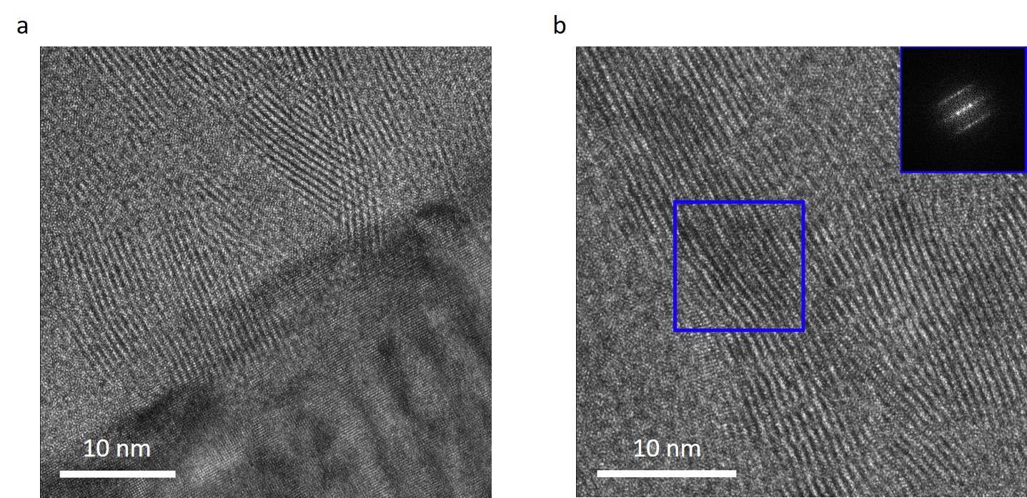
High-resolution TEM (HR-TEM) analysis was used to complement the information provided by the 3D FIB tomography. Figure 3a shows a HR-TEM image of the v-MoS2 nanosheets taken at the MoS2 and Mo-metal interface, where the vertical orientation of the nanosheets is unambiguous. This analysis also displays the same elongated vertical grains in the Mo-metal that were observed in the FIB tomography reconstruction (Figure 2). These findings indicate that the elongated Mo-metal grains formed during the metal deposition promote the vertical growth of the MoS2 nanosheets. The interlayer distance measured from the HR-TEM images (Figure 3b) turns out to be 0.65 nm, in agreement with previously reported values [19].
Figure 3 HR-TEM images of the MoS2/Mo-metal interface (a) and the v-MoS2 nanosheets (b).
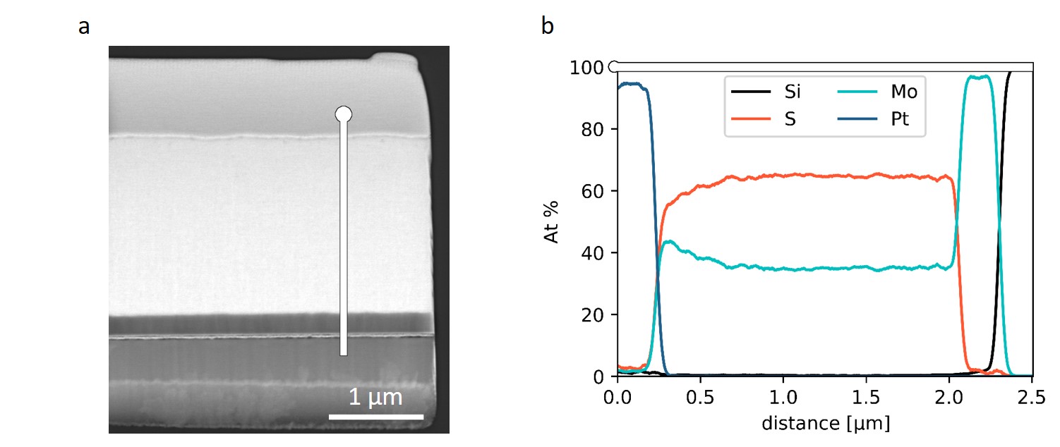
Further confirmation of the complete sulfurization of the Mo-metal is provided by chemical characterization using energy-dispersive X-ray spectroscopy (EDX). Figure 4a shows a high angle annular dark-field (HAADF) image of a TEM lamella fabricated from the sample in figure 1b. By performing an EDX linescan along the indicated line, we can determine the chemical composition of the different layers. The atomic percent (At%) of the different materials is displayed in figure 4b, indicating a 1:2 ratio between the Mo and S atoms along the entire linescan. From this profile, we can also accurately measure the thickness of the MoS2 layer to be 1.8 µm and the thickness of the remaining Mo-metal layer to be 0.26 µm. By varying the growth parameters and measuring the resulting MoS2 layer thickness one can also determine both the diffusion constant and the activation energy of this sulfurization process [15].
Figure 4 (a) HAADF image and (b) an EDX linescan displaying the At% along the TEM lamella.To summarize, we have exploited 3D FIB tomography and HR-TEM to characterize the vertical orientation of MoS2 nanosheets grown from the sulfurization of a pre-deposited Mo-metal layer. The chemical analysis provided by EDX enabled us to accurately measure the thickness of MoS2 and Mo-metal layers. Our results represent a comprehensive investigation of the growth mechanisms of v-MoS2 nanosheets [20].
- References
[1] M. Tinoco, L. Maduro, M. Masaki, et al., Nano Lett., vol. 17, no. 11 (2017), pp. 7021–7026.
[2] S. H. Gong, F. Alpeggiani, B. Sciacca, et al., Science, vol. 359, no. 6374 (2018), pp. 443–447.
[3] Z. Sun, A. Martinez, and F. Wang, Nature Photonics, vol. 10, no. 4. (2016), pp. 227–238.
[4] A. Autere, H. Jussila, Y. Dai, et al., Advanced Materials, vol. 30, no. 24. (2018) p. 1705963.
[5] A.-P. Luo, M. Liu, X.-D. Wang, et al., Photonics Res., vol. 3, no. 2 (2015), p. A69.
[6] X. Yin et al. Science, vol. 344, no. 6183 (2014), pp. 488–490.
[7] Y. Yu, C. Li, Y. Liu, et al., Sci. Rep., vol. 3 (2013), pp. 1–6.
[8] K. Kang et al., Nature, vol. 520, no. 7549 (2015), pp. 656–660.
[9] Y. Zhan, Z. Liu, S. Najmaei, et al., Small, vol. 8, no. 7 (2012), pp. 966–971
[10] N. Choudhary, J. Park, J. Y. Hwang, et al., ACS Appl. Mater. Interfaces, vol. 6, no. 23 (2014) pp. 21215–21222.
[11] Y.-H. Lee et al., Adv. Mater., vol. 24, no. 17 (2012), pp. 2320–2325.
[12] S. Najmaei et al., Nat. Mater., vol. 12, no. 8 (2013), pp. 754–759.
[13] D. Kong et al., Nano Lett., vol. 13, no. 3 (2013), pp. 1341–1347.
[14] Y. Jung, J. Shen, Y. Liu, et al, Nano Lett., vol. 14, no. 12 (2014), pp. 6842–6849.
[15] M. Bolhuis, J. Hernandez-Rueda, S. E. van Heijst, et al., arXiv:2001.10513 (2020).
[16] A. G. Dirks, R. A. M. Wolters, and A. E. M. De Veirman, Thin Solid Films, vol. 208, no. 2 (1992), pp. 181–188.
[17] J. A. Thornton, J. Vac. Sci. Technol. A Vacuum, Surfaces, Film., vol. 4 (1986), pp. 3059–3065.
[18] T. Sermpeniadi, MSc thesis, Delft University of Technology (2020)
[19] H. Li et al., Adv. Funct. Mater., vol. 22, no. 7 (2012), pp. 1385–1390.
[20] M.B., S.E.v.H., and S.C.-B. acknowledge financial support from ERC through the Starting Grant “TESLA” grant agreement No. 805021