Influence of thin AlAs capping layers on the structural and compositional properties of InAs QDs
- Abstract number
- 600
- Event
- Virtual Early Career European Microscopy Congress 2020
- Presentation Form
- Submitted Oral
- DOI
- 10.22443/rms.emc2020.600
- Corresponding Email
- [email protected]
- Session
- PSA.3 - Semiconductors & Devices
- Authors
- Ms Nazaret Ruiz Marín (1), Mr Daniel Fernández Reyes (1), Ms Sara Flores Gallegos (1), Ms Teresa Ben Fernández (1), Mr Lazar Stanojevic (2), Mr Alejandro Gallego Carro (2), Ms Alicia Gonzalo (2), Mr José María Ulloa (2), Mr David González (1)
- Affiliations
-
1. Universidad de Cádiz
2. Universidad Politécnica de Madrid
- Keywords
AlAs capping layers
InAs wetting layers
quantum dots
- Abstract text
SUMMARY
The structural features of the use of thin capping layers (CLs) of AlAs to implement in InAs quantum dot solar cells (QDSC) is investigated. On one hand, our results from EDX spectroscopy at the atomic scale contradict the hypothesis of a removal of the wetting layer (WL) during AlAs capping that should increase the open current voltage in QDSCs. Instead, we have observed an almost overlapping from the first monolayers (MLs) of the AlAs and InAs profiles that masks the contrast of the InAs WL at lower magnifications. On the other hand, the average QD size, areal density and In content, which have a clear interrelationship with the characteristics of the resulting WL, were determined by a combination of EDX, EELS and ADF measurements. The QDs show an almost linear increase of the In composition with the number of MLs of the AlAs layer following an Ostwald ripening-like behavior.
INTRODUCTION
Low dimensional nanostructures such as InAs QDs have been proposed as a means of implementing the intermediate band concept in QDSCs due to their discrete density of states and the maturity of the technology. However, for its success, several issues such as the thermal decoupling between the QDs and the conduction band of the WL needs to be overcome. A possible solution is the use of thin AlAs CL since it has been proposed that could reduce the WL effect because of the substitution of In by Al atoms1. In addition, AlAs should accumulate on top of the QDs, resulting in larger QD size and avoiding the In migration to the WL2. In this work, we have studied these effects using different thickness of AlAs CLs on InAs QDs by means of state-of-the-art structural and compositional TEM and STEM-related techniques.
MATERIALS AND EXPERIMENTAL DETAILS
A sample consisting in 5 QD layers with 2.7 monolayers (MLs) of InAs on (100) n+ GaAs substrate was grown by solid source molecular beam epitaxy. The QD layers were capped respectively with different thin AlAs CLs (0, 1, 2, 3 or 5 ML) followed by 50 nm GaAs. Diffraction contrast (DC) TEM analyses were carried out in a FEI Talos F200X. Annular dark field (ADF)-STEM imaging, energy dispersive X-Ray spectroscopy (EDX) with ChemiSTEM technology and low-loss electron energy loss spectroscopy (EELS) analyses were performed simultaneously in a FEI Titan Cubed3 Themis.
RESULTS AND DISCUSSION
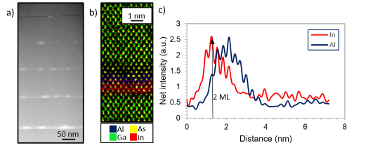
Certainly, the analysis by DCTEM using chemical sensitive g200 DF conditions and ADF imaging (Fig. 1a) evidences a gradual contrast fading of the InAs WL as the thickness of AlAs CL increases being finally almost replaced by that of AlAs itself. It seems to point to the suggested progressive substitution of the In atoms in the WL by the deposited Al1. However, EDX analysis at the nanometer scale demonstrates that Al atoms do not substitute In atoms but there is no hard interaction between them. In fact, there is an In/Al distribution overlapping from the second monolayer of the WL that hides the presence of the WL when using DCTEM or ADF imaging techniques (Fig. 1c).
Figure 1. (a) ADF image of the 5 layers. The contrast of regions between QDs (WL) changes from brighter (without AlAs) to darker (5 ML of AlAs) respect to GaAs regions. (b) Atomic resolution EDX map of the WL with 3 ML of AlAs. (c) Average EDX profiles of In and Al along the growth direction of (b). Al signal is observed from the 2nd InAs layer.
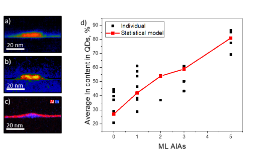
On the other hand, the size, composition and density of QDs are evaluated since they are key properties in the efficiency of QDSCs. First, a statistical study of the size of several dozens of QDs was carried out using color LUT ADF images where the criterion to size measurement were previously calibrated by comparing to EDX maps (Fig. 2 (a-c)). A significant increase of the QD heights with the AlAs thickness is found. Second, QD densities were estimated by combining the dot statistics with thickness measurements from low loss EELS maps. An inverse relationship is noticed between the average volume and the QD densities that points to a kind of Ostwald ripening process. The mean volume and density of the QDs together to measurements of the In content in the WL allowed us to calculate a statistical value of the average In content in QDs for each layer3. The estimated results show a linear increase of In content with the thickness of the AlAs layers. Indeed, In content values for individual QDs obtained by combining EDX measurements with EELS thickness maps are in agreement with the model (Fig. 2d). Nevertheless, the large increase of the In content of the QDs has a limited influence in the reduction of the WL because of the decay in the QD density by a ripening process.
Figure 2. ADF images (thermal LUT) corresponding to QDs without (a) and with (b) 5 ML of AlAs in the CL. (c) In and Al EDX map corresponding to a QD capped with 3 ML of AlAs. (d) Average In content of individual QDs (black squares) and the one obtained by the statistical model (red line) for the different layers.
- References
1. Tutu, F. K. et al. InAs/GaAs quantum dot solar cell with an AlAs cap layer. Appl. Phys. Lett. 102, 163907 (2013).
2. Tsatsul’nikov, A. F. et al. Volmer-Weber and Stranski-Krastanov InAs-(Al,Ga)As quantum dots emitting at 1.3 μm. J. Appl. Phys. 88, 6272–6275 (2000).
3. Gonzalez, D. et al. Quantitative analysis of the interplay between InAs quantum dots and wetting layer during the GaAs capping process. Nanotechnology 28, 425702 (2017).