Interfacial interaction and structural evolution in Ge-Sn nanofilms
- Abstract number
- 922
- Event
- European Microscopy Congress 2020
- DOI
- 10.22443/rms.emc2020.922
- Corresponding Email
- [email protected]
- Session
- PSA.2 - Metals & Alloys
- Authors
- Alexey Minenkov (1, 2), Tia Truglas (1), Heiko Groiss (1)
- Affiliations
-
1. Christian Doppler Laboratory for Nanoscale Phase Transformation, Center for Surface and Nanoanalytics, Johannes Kepler University Linz
2. School of Physics and Technology, V.N. Karazin Kharkiv National University
- Keywords
Ge-Sn, in situ TEM, metal-induced crystallization of semiconductors, phase transformations, size effect, thin films
- Abstract text
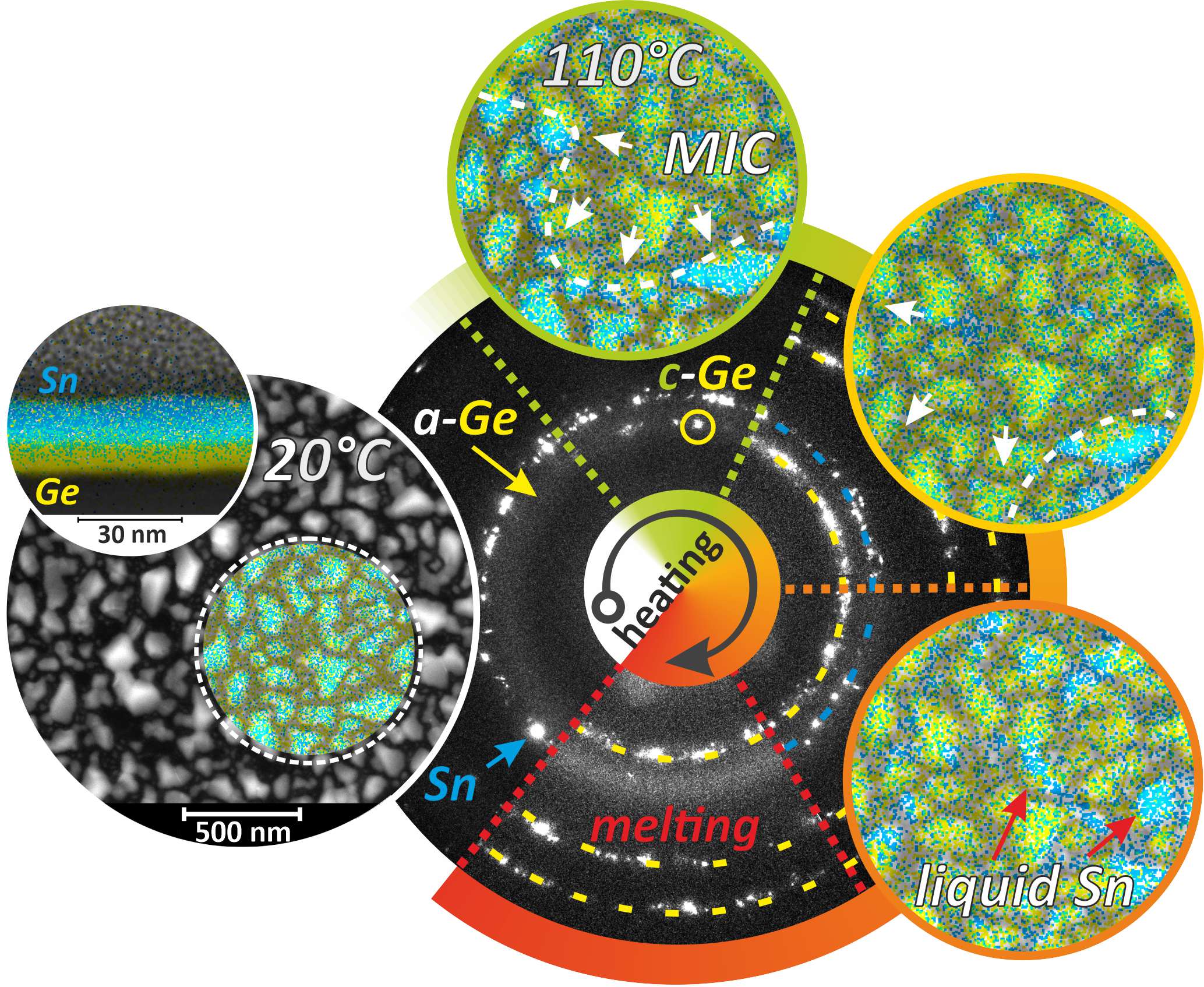
The progressing complexity of modern electronics and the ongoing miniaturization of semiconductor engineering motivate us to untiringly search for stable and efficient nanomaterials with advanced pre-desired properties. In this regard, metal-semiconductor systems look exceedingly promising. The applications of these systems range from lead-free solders and ohmic contacts with minimal, thermally-stable resistance (Au-Ge, Ag-Ge) to the monolithic integration of the state of the art light emitters. For the latter, a number of authors (e.g. [1-2]) have demonstrated the prospect of using the Ge-Sn binary system compatible with Si. Adding tin to germanium makes it possible to create a direct semiconductor material, the concentration of tin wherein should be more than 8 at.% [2]. It’s noteworthy though that this value significantly exceeds the known equilibrium bulk solubility of Sn in Ge. Despite the considerable applied interest, peculiarities of components interaction and the stability of the Ge-Sn system while heat-treating are still far from a full understanding, especially at the nanoscale.
We address this problem in a frame of comprehensive in situ TEM investigation of melting-crystallization phase transitions and interfacial interactions in Ge-Sn nanofilms. We have used the series of thin layered Ge-Sn films formed via sequential thermal evaporation and MBE as a convenient model of equilibrium and non-equilibrium nano-binaries, respectively. It should be additionally mentioned, that Ge being formed at room temperature using thermal evaporation is amorphous (a-Ge). The morphological and structural evolution of the samples was painstakingly traced in real-time during heating-cooling cycles (20 - 300°C) performed directly in JEOL JEM - 2200FS TEM equipped with MEMS-based Wildfire heating-holder provided by DENSsolutions. A combination of complementary microscopic techniques (HRTEM, HAADF STEM, SAED) in conjunction with plain-view and cross-sectional EDX elemental mapping allows us to establish the liquid phase formation and crystallization temperatures on the fly in a single experiment. In addition, we have also varied the characteristic thickness of the samples in the 5 - 50 nm range to define the effect of size on investigated processes. The principal attention was given to a phenomenon of metal-induced crystallization (MIC) of amorphous germanium in contact with tin. In particular, it was found that the MIC temperature in the system under study could be as low as 110°C. Our previous results [3-4] give us the ground to predict that the aforementioned value corresponds also to the onset temperature of liquid phase formation at the metal-semiconductor interface. New data on the MIC impact on the samples’ morphology will be also presented and discussed [5].
- References
[1] D Stange et al, ACS Photonics 2 (2015), p. 1539
[2] MS Seifner, S Hernandez, J Bernardi, A Romano-Rodriguez, and S Barth, Chem. Mater. 29 (2017), p. 9802
[3] AA Minenkov, AP Kryshtal and SI Bogatyrenko, Journal of Alloys and Compounds 756 (2018), p. 50
[4] A Kryshtal, A Minenkov, S Bogatyrenko, and A Gruszczynski, Journal of Alloys and Compounds 786 (2019), p. 817
[5] We would like to gratefully acknowledge the financial support by the Austrian Federal Ministry for Digital and Economic Affairs and the National Foundation for Research, Technology and Development in the frame of the Christian Doppler Laboratory for Nanoscale Phase Transformations.