Investigation of dynamic processes in Janus particle-seeded III-V semiconductor nanowires
- Abstract number
- 238
- Event
- Virtual Early Career European Microscopy Congress 2020
- Presentation Form
- Submitted Oral
- DOI
- 10.22443/rms.emc2020.238
- Corresponding Email
- [email protected]
- Session
- PSA.3 - Semiconductors & Devices
- Authors
- Michael S. Seifner (1, 2), Markus Snellman (2, 3), Daniel Jacobsson (1, 2, 4), Knut Deppert (2, 3), Maria E. Messing (2, 3), Kimberly A. Dick (1, 2, 3)
- Affiliations
-
1. Centre for Analysis and Synthesis, Lund University
2. NanoLund, Lund University
3. Solid State Physics, Lund University
4. National Center for High Resolution Electron Microscopy, Lund University
- Keywords
In situ TEM, Nanowire, Janus particle, Nucleation, Growth dynamics, Interfaces
- Abstract text
The dynamic processes occurring during the nucleation and growth of III-V semiconductor nanowires seeded via two-phase Ag-Cu particles are in the focus of in situ transmission electron microscopy (TEM) investigations. For that purpose, particular attention is paid to the origin of the nucleation, the step-flow growth of bilayers forming the nanocrystal, the elemental distribution, and the epitaxial relations between the solid components.
A wide range of different metals promoting the anisotropic growth of III-V semiconductor nanostructures can be found in literature.[1] In general, metal seeds have the potential to alter the physical properties of a nanowire by triggering the formation of a metastable phase,[2] incorporating foreign atoms from the metal seed in the nanowire host lattice,[3] favouring growth in uncommon growth directions,[4] and transferring defects from the seed into the nanowire crystal.[5] Nevertheless, some of these processes, e.g. the formation of deep level traps in Si nanowires via the incorporation of atoms from the Au seed in the Si crystal,[6] are not desired and deteriorate the physical properties of a material. Therefore, the investigation of dynamic processes in crystal growth and the influence of synthesis parameters is of high importance for the semiconductor industry, which aims for tailoring the physical properties of a nanomaterial to be applicable in devices.
The mechanisms of metal-seeded nanowire growth performed in the gas phase can be divided into the vapour-liquid-solid (VLS) and the vapour-solid-solid (VSS) approaches, which describe the state of the present phases during growth conditions.[7] The state of the seed during the growth process is an important criterion for characterising the transport pathways of atomic species towards the growth front of a nanowire. However, there remain many open questions concerning the growth mechanism for both VLS and VSS growth of semiconductor nanowires and various parameters including the involved phases / elements and synthesis conditions have to be taken into account.
The growth of III-V semiconductor nanowires using solid Ag[8] and Cu[9] seeds is already reported in literature; however, Ag-Cu Janus particles and two-phase seed particles in general have not been considered as growth promoter so far. The motivation of this study is the potential introduction of additional possibilities for tuning nanowire properties by the controlled incorporation of defects using two-phase particles as growth seeds.
For that purpose, Ag-Cu Janus particles produced in a spark discharge generator are deposited on a SiNx-coated heating chip for in situ TEM investigations. Subsequently, the chip is transferred into an environmental TEM (ETEM) with the possibility to add metal-organic precursors. A detailed description of the used setup can be found elsewhere.[10] Chemical vapour deposition is performed at the heated area of the chip and the processes are traced by high-resolution bright-field imaging with aberration correction, electron diffraction, high-angle annular dark-field (HAADF) scanning transmission electron microscopy (STEM), and energy dispersive X-ray (EDX) measurements.
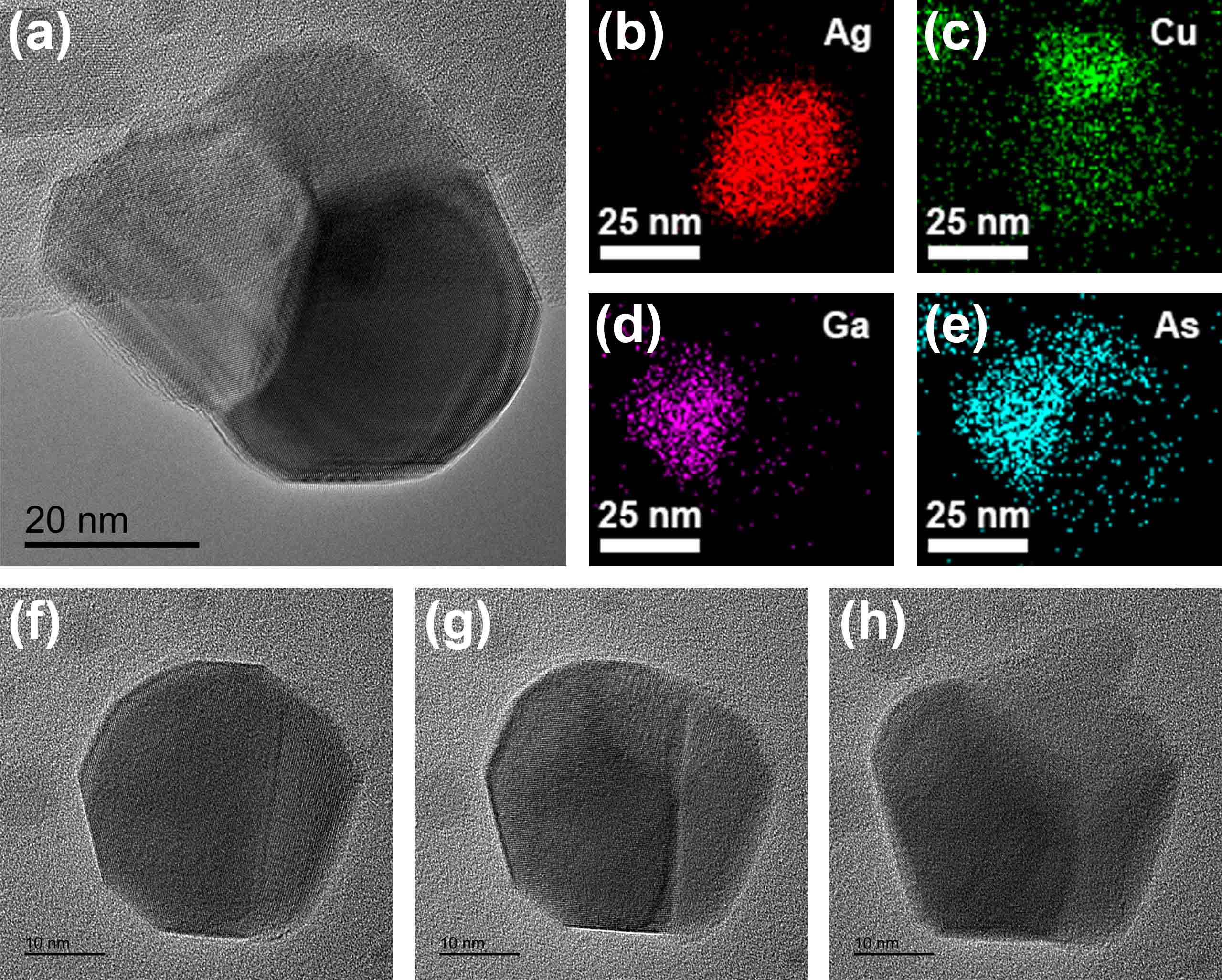
Initial experiments are focused on the behaviour of Ag-Cu particles under different conditions and atmospheres. Moreover, the influence of further elements of group III / V added to the binary system are investigated. The controlled switching between different morphologies of the seed particle is a major finding in this study. The elemental distribution at an early stage of GaAs nucleation is shown in Figure 1a-e and suggests enrichment of As in Cu. The origin of GaAs nucleation is mainly observed at the solid-solid interface of a Ag-Cu Janus particle, which is highlighted in Figure 1f-h. Representative frames of an in situ TEM movie acquired during the supply of arsine (AsH3) and trimethylgallium (TMGa) in the presence of a Ag-Cu Janus particle at elevated temperatures suggest the (f+g) formation of the GaAs nucleus at the triple phase boundary of the Janus particle and (h) a subsequent rearrangement of the components. Furthermore, first analyses point towards the possibility to transfer the solid-solid interface of the Janus particle into the nanowire crystal.
Figure 1. (a-e) STEM-EDX measurements on a structure obtained at an early stage of the nucleation process shown in (a) reveal the elemental distribution of (b) Ag, (c) Cu, (d) Ga, and (e) As. Enrichment of As in Cu is clearly visible in (c+e) suggesting the presence of a Cu-As alloy during nucleation. (f-h) The chronological steps of the nucleation process of GaAs nanowires using a Ag-Cu Janus particles as growth promoter are highlighted by representative frames of an in situ TEM movie. (f) shows a Janus particle with a Ag- (left) and Cu-rich part (right). (g) Nucleation at the triple phase boundary of the Janus particle is observed after the supply of both precursor species. (h) Rearrangement of the different phases occurs, once a GaAs nucleus is formed.
The conscious use of two-phase particles for metal-seeded nanowire growth is presented in this conference contribution. A deeper understanding of nucleation and growth of nanowires using two-phase solid seed particles is obtained and a novel approach for the controlled formation of defects in nanostructures to tailor the physical properties is introduced. This proof of concept for Janus particle-seeded nanowire growth has the potential to pave the way for a new approach to manipulate physical properties at the nanoscale in a controlled manner.[11]
- References
[1] K. A. Dick and P. Caroff, Nanoscale 6 (2014), p. 3006.
[2] J. Tang et al, Nanoscale 9 (2017), p. 8113.
[3] M. S. Seifner et al, ACS Nano 13 (2019), p. 8047.
[4] E. C. Garnett et al, Advanced Materials 19 (2007), p. 2946.
[5] S. Barth et al, Nano Letters 11 (2011), p. 1550.
[6] E. Koren et al, Nano Letters 11 (2011), p. 2499.
[7] P. C. McIntyre and A. Fontcuberta i Morral, Materials Today Nano 9 (2020), p. 100058.
[8] A. T. Vogel et al, Nanotechnology 22 (2011), p. 015605.
[9] K. Hillerich et al, Journal of Crystal Growth 315 (2011), p. 134.
[10] C. Hetherington et al, Semiconductor Science and Technology 35 (2020), p. 034004.
[11] The authors gratefully acknowledge financial support from the Knut and Alice Wallenberg Foundation (KAW).