Limitation of power-law model for STEM Z-contrast
- Abstract number
- 825
- Event
- European Microscopy Congress 2020
- DOI
- 10.22443/rms.emc2020.825
- Corresponding Email
- [email protected]
- Session
- PSA.1 - 1D & 2D Materials
- Authors
- Dr. Koji Kimoto (2), Dr. Shunsuke Yamashita (2), Dr. Kazuo Ishizuka (1)
- Affiliations
-
1. HREM Research Inc.
2. National Institute for Materials Science
- Keywords
ADF, STEM, Z contrast
- Abstract text
Annular dark-field (ADF) imaging by scanning transmission electron microscopy (STEM) is a common technique for material characterization with high spatial resolution. Major advantages of ADF imaging are its intuitive contrast and atomic sensitivity, and the atomic number dependence of ADF signal has been investigated since a pioneering study by Crewe et al. It has been reported that ADF signal is proportional to the n-th power of the atomic number Z [1,2], i.e., the power-law model of the Z contrast. In this study we reexamine the limit of the power-law model by performing experiments and simulations.
ADF signal can be quantitatively analyzed as the scattering probability of incident electrons [3]. We quantitatively observed ADF images of monolayer graphene, in which the ADF signal was quantified as the number of electrons [4-6]. Since 2D materials are ideal standard specimens with known thicknesses, we have applied the quantitative ADF imaging for graphene, MoS2 and WS2 nanosheets.
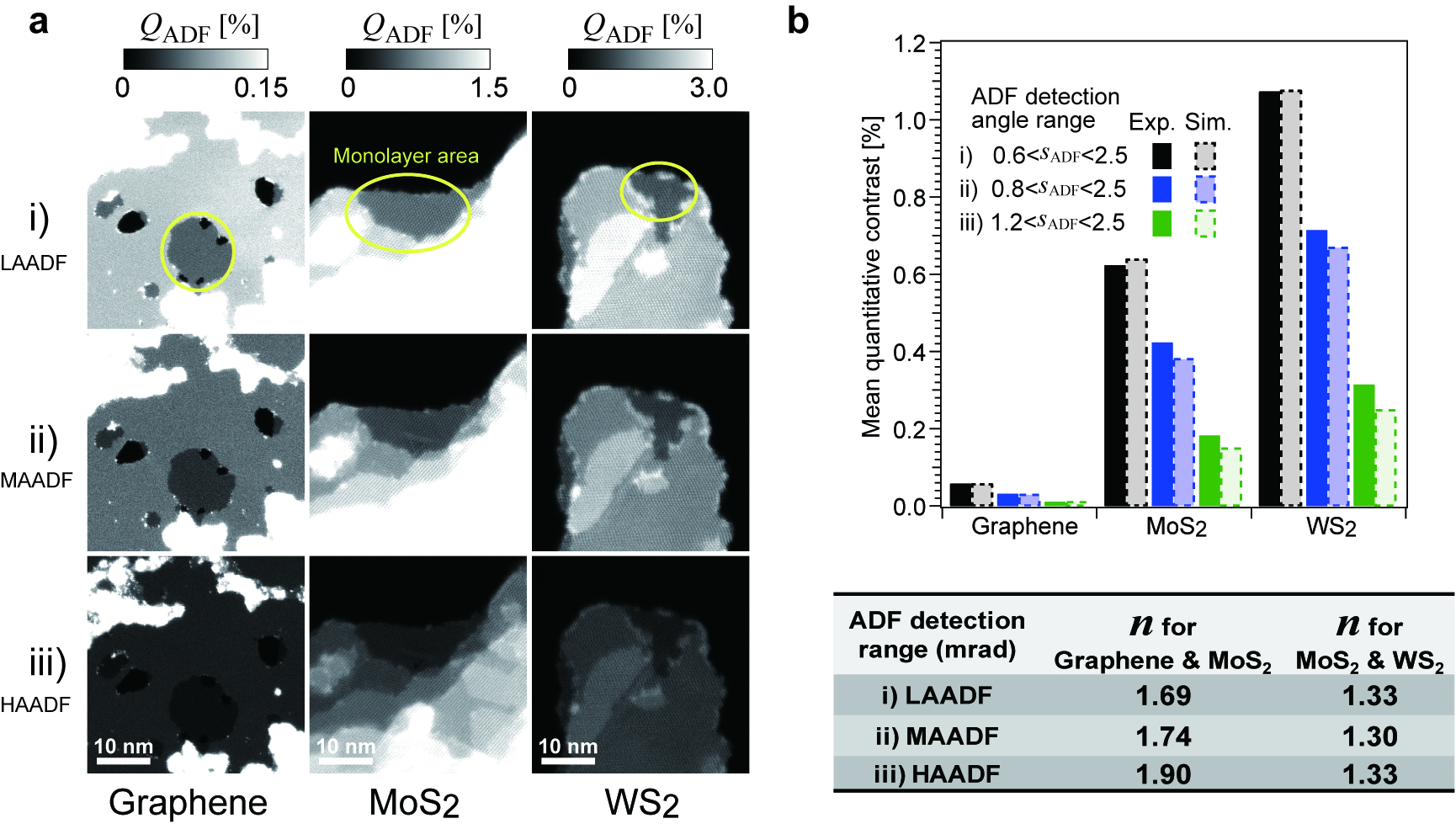
Figure 1 shows quantitative ADF images under various scattering angle ranges. Quantitative ADF images of the 2D materials and the averaged ADF signal of each monolayer are shown in Figs. 1a and 1b, respectively. Although the microscope can resolve individual atoms, here we discuss the spatially averaged ADF signal, which is experimentally reproducible. It is found that the power-law model is not always valid as shown in the table in Fig. 1b.
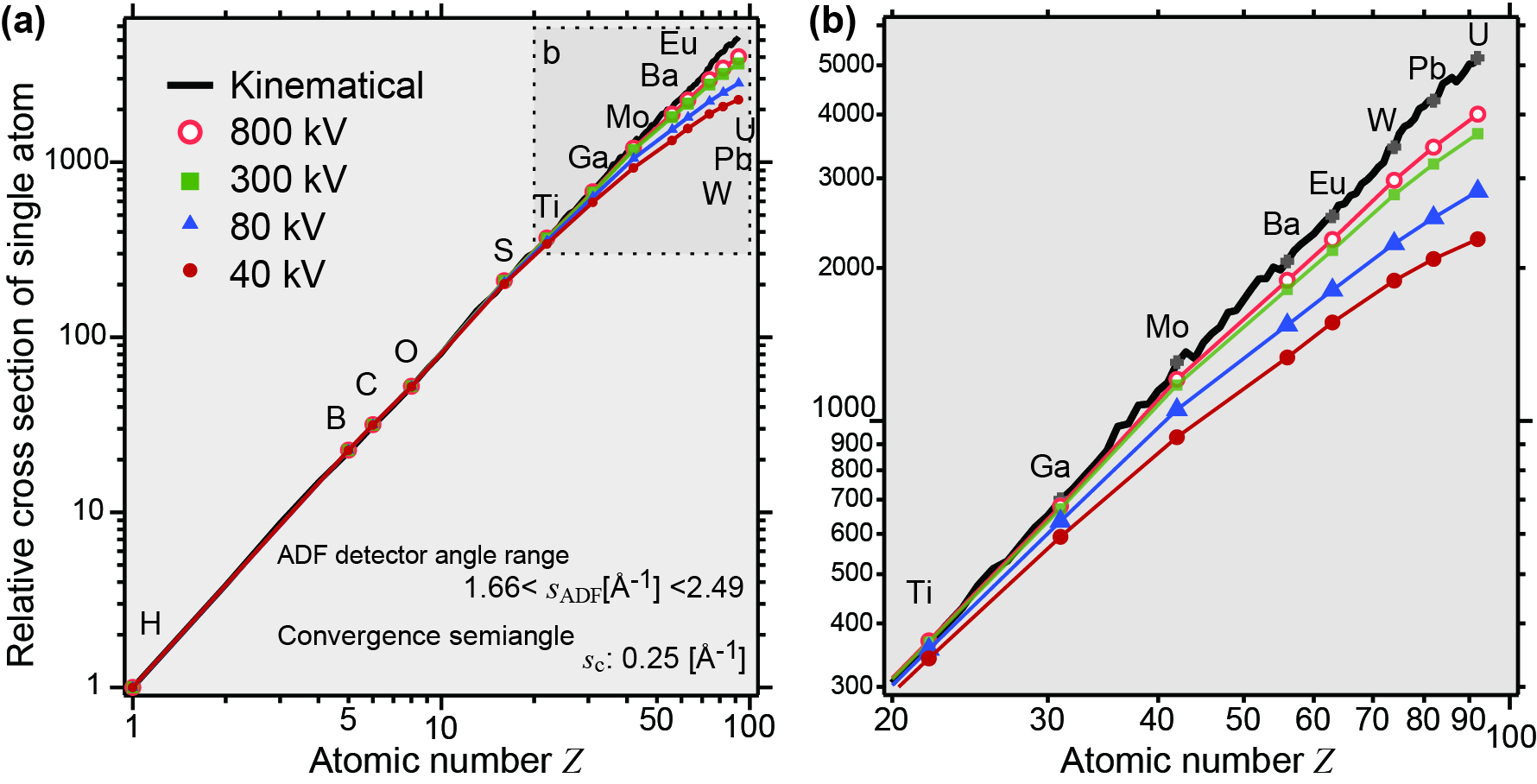
Next, we investigate the ADF signal by performing phase-object simulations (HREM Research Inc. xHREM). The cross section of each atom is evaluated as the integrated scattering intensity of the ADF image. Since the atomic potentials are sharp in real space, simulations that include a high frequency of up to scattering parameter s=25 [Å-1] must be performed. The cross section of each single atom has been normalized by that of H atom (Fig. 2). The almost straight line representing the kinematical calculation in the log-log plot indicates the validity of the power-law model. However, the phase-object simulation shows that there is a systematic deviation, particularly for high-Z elements, at a lower acceleration voltage. The deviation becomes evident for many elements (Z>20) as shown in Fig. 2b. This is due to the coherent strong scattering of incident electrons, i.e., a limit of the first Born approximation. Although the deviation is not negligible even at a high acceleration voltage (e.g., 300 kV) and high scattering angle, quantitative analysis can be performed on the basis of the accurate phase-object simulations.
Figure 1 Experimental ADF images of 2D materials and spatially averaged ADF contrast of each monolayer. (a) ADF images of the 2D materials (graphene, MoS2 and WS2) observed under three camera lengths at 80 kV. (b) Averaged ADF contrast of each monolayer under the three experimental conditions. Experimental results and the results of phase-object simulations are shown by bars with solid and broken lines, respectively.
Figure 2 Atomic number dependence of integrated ADF contrast of single atoms. (a) Z dependence of the integrated ADF contrast, which is normalized by that of a hydrogen atom and (b) enlarged graph. Marks show the results of phase-object simulations and the black line represents the kinematical calculation. Note the breakdown of the power-law model, i.e., deviation from the straight line in the log-log graph, particularly for heavy elements, at lower acceleration voltages.
- References
[1] O.L. Krivanek, et al., Nature 464 (2010) 571-574.
[2] E.J. Kirkland, Advanced Computing in Electron Microscopy, Second Ed, Springer, New York, 2010.
[3] J.M. LeBeau and S. Stemmer, Ultramicroscopy 108 (2008) 1653-1658.
[4] S. Yamashita, et al., Microscopy 64 (2015) 409-418.
[5] S. Yamashita, et al., Microscopy 64 (2015) 143-150.
[6] S. Yamashita, et al., Sci. Rep. 8 (2018)