Low-dose Scanning Transmission Electron Microscopy Methods to Obtain High-Resolution Information of Pharmaceutical Organic Crystals
- Abstract number
- 902
- Event
- European Microscopy Congress 2020
- DOI
- 10.22443/rms.emc2020.902
- Corresponding Email
- m.s.s'[email protected]
- Session
- PST.5 - Diffraction techniques and structural analysis
- Authors
- Dr Mark S'ari (1), Natalia Koniouch (1), Dr James Cattle (1), Dr Nicole Hondow (1), Prof Rik Brydson (1), Dr Andy Brown (1)
- Affiliations
-
1. University of Leeds
- Keywords
Diffraction, Low-dose, Organic Crystal, Pharmaceuticals,
- Abstract text
In oral drug delivery, drug solubility and dissolution are the rate-limiting factors in achieving the desired pharmacological response, with more than 40% of drugs currently in development classified as poorly water-soluble [1]. To improve bioavailability of a drug many solubilisation technologies have been developed, one of which is solid dispersion, where an amorphous active pharmaceutical ingredient (API) and polymer are chemical or physically mixed. An amorphous drug is more soluble than its crystalline form, however, it is thermodynamically unstable and will tend to crystallise. Addition of a polymer can kinetically stabilise an amorphous drug or API within the polymer matrix increasing bioavailability [2]. If crystallisation does occur solubility and dissolution rates of an API can decrease leading to lower bioavailability and further recrystallisation. It is therefore of value to characterise an API after processing and during the shelf-life of the final product.
The use of TEM to characterise organic crystals offers increased spatial resolution and detection limits compared to other conventional techniques. However, organic compounds are easily damaged when irradiated by the electron beam causing destruction of crystallinity and structural changes. Therefore the total applied electron dose or fluence must be limited to reduce any damage to preserve crystallinity and enable its identification. Here we report on the use of scanning electron diffraction (SED) as a tool to identify and quantify the number of areas that are crystalline within solid dispersions to detect the early onset of recrystallization. We also report on the use of TEM and STEM scanning moiré fringes (SMFs) to crystal lattice images to identify defects. Previously established fluence limits were taken into considering throughout this work [3].
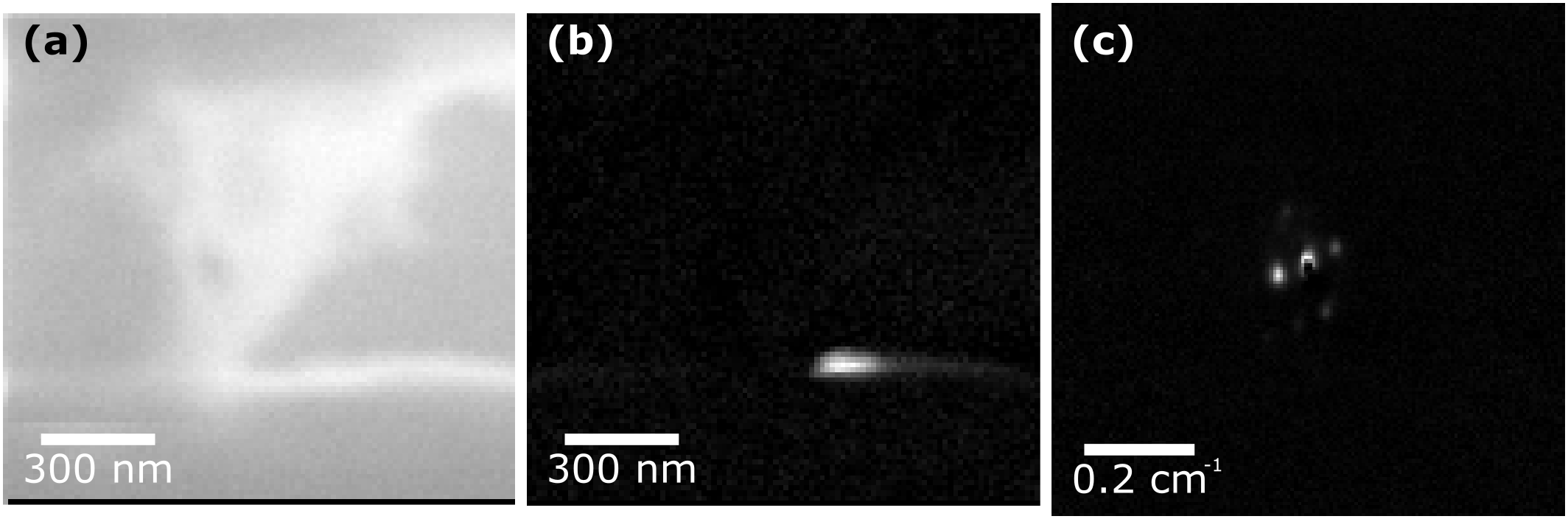
An FEI Tecnai F30 operated at an accelerating voltage of 300 kV with scanning and precession of the electron beam controlled by a DigiSTAR Nanomegas was used to collect SED data on a solid dispersion of felodipine and PVP/VA in a 50:50 ratio prepared by hot-melt extrusion. A 1 µm condenser aperture was inserted to provide a convergence angle of 1 - 2 mrad and to reduce the electron beam intensity, a scan step size of 10 nm and dwell time of 10 ms were used. The resulting 4D data contain 2D diffraction data at each point in the image and by using virtual apertures a reconstructed bright-field image of the scanned area can be obtained (Figure 1a). Non-negative matrix factorisation (NMF) was applied to identify crystalline regions by learning the component diffraction patterns in the data as well as the real space loading of each component. The resulting analyses showed that only one area ~75 x 150 nm within a ~ 900 x 900 nm scanned area of sample appeared crystalline (Figure 1b and 1c).
High-resolution TEM and SMFs images of furosemide were collected on an FEI Titan3 Themis G2 operated at 300 kV and equipped with a monochromator. High-resolution TEM images were collected at an electron flux of 10 e-/Å2 s with a total electron fluence of 10 e-/Å2 resulting in the observation of 0.46 nm and 0.49 nm lattice fringes, however, the fringes were only visible in a few small areas across the whole crystal suggesting the other areas had been damaged by the electron beam.
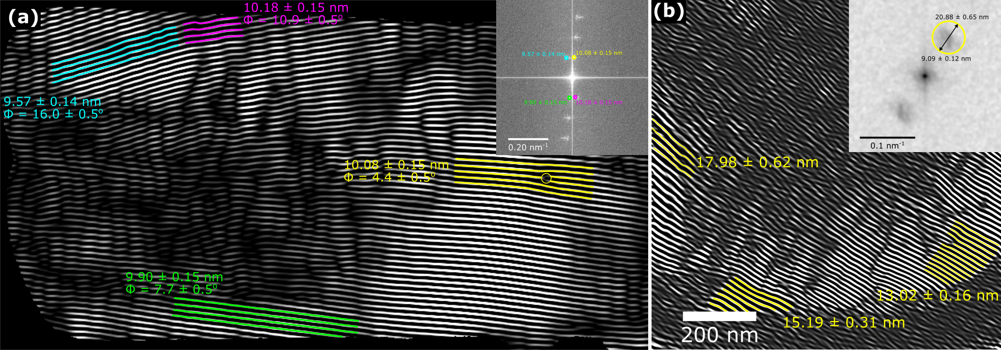
SMFs were acquired by identifying areas containing strongly diffracting crystal regions in TEM [4]. The microscope was then operated in STEM and aligned. The scan direction was rotated to align with the direction of the desired crystal lattice planes. The magnification was selected so that the pixel size was similar to the size of the aligned d-spacings, for the (001) spacings in furosemide a pixel size of 1.32 nm was used with the d-spacing being equal to 1.50 nm (Figure 2a). Similarly, the (010) spacing was imaged using a pixel size of 0.93 nm and d-spacing of 0.96 nm (Figure 2b). This resulted in a total electron fluence per image of 1.8 e-/Å2 and 3.6 e-/Å2 for the (001) and (010) d-spacings respectively. Images of the (001) d-spacing showed that several of the SMFs observed had minor variations in size and angle, suggesting strain due to defects within the crystal. Likewise, in the images of the (010) d-spacing, there were variations in the measured and predicted size and angle of the SMFs, however, here the variations were much larger suggesting increased amounts of strain and defect density within the (010) planes [5]. This may relate to measured differences in crystal face dissolution rates in furosemide [6].
Both SED and STEM SMFs appear to be promising techniques for the analysis of pharmaceuticals by TEM. These techniques can improve understanding of crystallization pathways in organic compounds, degradation in pharmaceutical formulations and the effect of defects on dissolution rate of different crystal faces.
Figure 1: (a) Reconstructed BF image (b) real spacing loading of NMF (c) component diffraction pattern of NMF of a felodipine PVP 50:50 solid dispersion.
Figure 2: Furosemide crystal analysis (a) Fourier filtered SMF image of (001) d-spacings at 1.50 nm and 1.32 nm pixel size taken at a total fluence of 1.8 e-/Å2 (b) Fourier filtered SMF image of (010) d-spacings at 0.96 and 0.93 nm pixel size taken at a total fluence of 3.6 e-/Å2.
- References
[1] Kanaujia et. al. Powder Technol. 2015, 285, 2-15.
[2] Bard and Taylor Adv. Drug Deliv. Rev. 2012, 64, 396-421.
[3] S'ari et al. Mol. Pharm. 2018, 15 (11), 5114-5123.
[4] S'ari et al. Micron 2019, 120, 1-9.
[5] S'ari et al. J. Microsc. 2020.
[6] Adobes-Vidal et al. Crystl. Growth Des. 2016 16, 4421-4429.