Magnetic Field Evaluation with Atomic Layer Resolution by Aberration-Corrected 1.2-MV Holography Electron Microscope
- Abstract number
- 457
- Event
- European Microscopy Congress 2020
- DOI
- 10.22443/rms.emc2020.457
- Corresponding Email
- [email protected]
- Session
- PSA.9 - Magnetic and Spintronic Materials
- Authors
- Dr. Toshiaki Tanigaki (1), Dr. Tetsuya Akashi (1), Mr. Takaho Yoshida (1), Dr. Ken Harada (5), Dr. Kazuo Ishizuka (2), Dr. Masahiko Ichimura (1), Prof. Yasukazu Murakami (5, 6), Dr. Kazutaka Mitsuishi (3), Dr. Yasuhide Tomioka (4), Prof. Daisuke Shindo (5, 8), Dr. Xiuzhen Yu (5), Pfor. Yoshinori Tokura (5, 7), Dr. Hiroyuki Shinada (1)
- Affiliations
-
1. Hitachi, Ltd.
2. HREM Research Inc.
3. National Institute for Materials Science
4. National Institute of Advanced Industrial Science and Technology (AIST)
5. RIKEN Center for Emergent Matter Science (CEMS)
6. Kyushu University
7. The University of Tokyo
8. Tohoku University
- Keywords
Electron holography, Phase imaging, Magnetic field observation
- Abstract text
Materials innovation requires understandings of not only structures but also electromagnetic fields in materials through analyzing the origins of functions. Electron holography is a powerful technique for observing electromagnetic fields at high resolution by capabilities of in-focused observations and post aberration corrections.
The development of an aberration corrected 1.2-MV holography electron microscope [1,2] has improved resolutions in electron holography. The TEM point resolutions of this microscope in the field-free mode is 0.24 nm [2]. For observing magnetic fields, we have to separate electrostatic and magnetic effects to the electron wave. To separate these two effects by reversing magnetization in the sample, we have developed a pulse magnetization system. Using the system, the magnetic fields were observed at 0.67-nm resolution [3]. However, due to the aberrations introduced in the experiments, the atomic-resolution has not been achieved. Here, we show the atomic-layer in-plane magnetic field analysis using post-aberration correction for reconstructed electron wave.
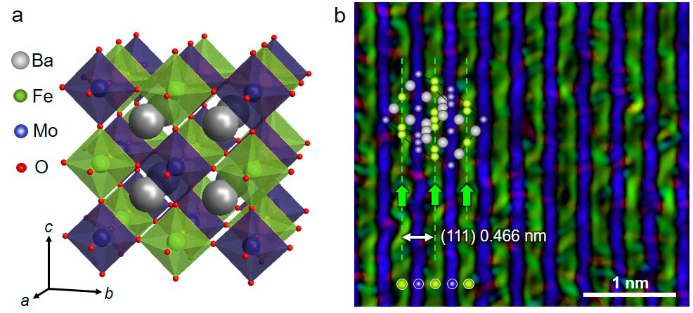
Figure 1(a) shows schematics of the crystal structure of Ba2FeMoO6 with double perovskite structure [4]. In the ferrimagnetic Ba2FeMoO6, Fe and Mo atoms have opposite magnetic moments. TEM thin samples with rectangular shape along with the (111) layer were prepared by using focused ion beam instruments. In this sample, the magnetization along (111) layer is formed by the shape effect. In the observation experiments, a pulse magnetic field of 207 kA/m was applied to reverse the sample magnetization. The hologram acquisitions were performed at room temperature without magnetic field. The experimentally introduced aberrations of C1, A1, C3, and C5 estimated by Thon diagrams [5] were corrected and averaged to increase the signal to noise ratios of the images. The phase images were aligned by using the non-magnetic surface carbon layer and the amplitude images, and then the phases were decomposed into the electrostatic and magnetic phases.
Figures 1(b) shows derivative of magnetic phase that reflects the in-plane magnetic field along (111) lattice. To indicate the atomic positions, the crystal models are overlapped onto the image. Note that the sample was tilted about 3 degree from [110] directional observation conditions while keeping (111) lattice parallel to the electron beam. Thus the atomic columns are not observed but (111) lattices are observed. By the multi-slice simulation including atomic-scale magnetic field derived by density functional theory calculations, it is shown that the observed result does reflect the atomic-layer in-plane magnetic field distributions.
On the basis of high resolution performance of aberration corrected 1.2-MV holography electron microscope, the atomic level magnetic filed observation has been realized by using the plus magnetization system and post aberration correction methods. We believe that the developed technologies can be used for varieties of applications from materials innovation to the developments of future devices.
References:
[1] T. Akashi et al., Appl. Phys. Lett. 106 (2015), p. 074101.
[2] T. Tanigaki et al., Adv. Imaging Electron Phys. 198 (2016), p. 69.
[3] T. Tanigaki et al., Sci. Rep. 7 (2017), p. 16598.
[4] Y. Tomioka et al., Phys. Rev. B 61 (2000) p. 442.
[5] Y. Takai et al., J. Electron Microsc. 47 (1998) p. 419.
Acknowledgments:
Development of the 1.2-MV holography electron microscope was supported by a grant from the Japan Society for the Promotion of Science (JSPS) through the “Funding Program for World-Leading Innovative R&D on Science and Technology (FIRST Program)” initiated by the Council for Science, Technology, and Innovation (CSTI). Part of this research was supported by JST CREST Grant Number JPMJCR1664, Japan.
Figure 1. (a) Crystal structure of Ba2FeMoO6. (b) Derivative of magnetic phase.