Magnetic field free atomic resolution STEM for magnetic materials
- Abstract number
- 459
- Event
- European Microscopy Congress 2020 Invited Speakers
- DOI
- 10.22443/rms.emc2020.459
- Corresponding Email
- [email protected]
- Session
- PST.3 - New Instrumentation
- Authors
- Professor Naoya Shibata (1)
- Affiliations
-
1. The University of Tokyo
- Keywords
DPC, magnetic materials, objective lens
- Abstract text
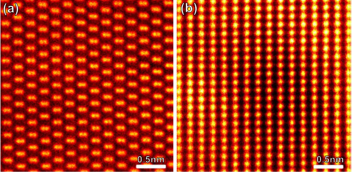
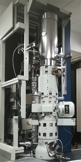
Aberration-corrected scanning transmission electron microscopy (STEM) is a powerful technique to directly observe atomic-scale structures and chemistry of individual defects, such as interfaces, inside materials and devices. In the state-of-the-art STEM, a probe size of less than 0.5Å in diameter has been experimentally realized [1]. Now, the following interesting question arises: beyond just atoms, what might become observable by using such fine electron probes? One answer to this question may come from exploring new possibilities in phase contrast imaging in STEM. By using elaborate detectors, we can not only image single atoms, but can also image electromagnetic field distribution of atoms through differential phase contrast (DPC) imaging techniques [2]. Applying DPC imaging in atomic resolution STEM [3], we can now directly visualize the electric field distribution within single atoms [4], i.e. the electric field between the positively charged atomic nucleus and the negatively charged electron cloud. It then becomes tempting to directly observe magnetic fields at atomic resolution, which should strongly correlate with the properties of magnetic materials and devices. However, atomic-resolution observation of magnetic materials is essentially very difficult by using conventional electron microscopes, because high magnetic fields (~2T) are always exerted on samples inside the magnetic objective lens. In recent years, we have developed a new magnetic objective lens system that realizes a magnetic field free environment at the sample position. Using this new objective lens system combined with the state-of-the-art higher order aberration corrector [5], direct atom-resolved imaging in a magnetic field free environment has been achieved [6]. Figure 1 shows an annular dark field STEM images of GaN single crystal and Fe-3%Si alloy, one of the most important engineering soft magnetic materials. This novel electron microscope (Magnetic-field-free Atomic Resolution STEM: MARS), shown in Figure 2, is expected to be used for research and development of advanced magnetic materials and devices. The details of this magnetic-field-free STEM and the material application results will be presented in the talk.
Figure 1: Atomic-resolution annular dark field STEM image of (a) GaN single crystal observed from [111] and Fe-3%Si alloy observed from the [110] direction [6]. In GaN, the Ga-Ga dumbbells of 0.92Å separation are clearly resolved in real space.The magnetic field at the sample position is kept well below 0.2mT.
Figure 2: The MARS microscope installed at the University of Tokyo.
- References
[1] S. Morishita et al., Microscopy, 67, 46 (2018).
[2] N.H. Dekkers and H. de Lang, Optik, 41, 452 (1974).
[3] N. Shibata et al., Nature Phys., 8, 611-615 (2012).
[4] N. Shibata et al., Nature Comm. 8, 15631 (2017).
[5] H. Sawada et al., J. Electron Microsc., 58, 341-347 (2009).
[6] N. Shibata et al., Nature Comm. 10, 2380 (2019).
[7] The author thank all the collaborators of this research, especially Y. Kohno, T. Seki, S. Morishita, A. Nakamura, H. Sawada, T. Matsumoto, S.D. Findlay and Y. Ikuhara. The author acknowledges support from the JST SENTAN Grant Number JPMJSN14A and the JSPS KAKENHI Grant number 19H05788.