Micro-manipulation of carbon nanocones for Scanning Probe Microscopy
- Abstract number
- 1440
- Event
- European Microscopy Congress 2020
- DOI
- 10.22443/rms.emc2020.1440
- Corresponding Email
- [email protected]
- Session
- PST.8 - Scanning Probe microscopy:imaging and beyond
- Authors
- Assistant Engineer Robin Cours (1), PhD student Germercy Paredes (1, 3), Engineer Grégory Seine (1), Doctor Etienne Palleau (2), Doctor Marc Monthioux (1)
- Affiliations
-
1. CEMES - CNRS
2. LPCNO - CNRS & INSA
3. Nanoscience Research Laboratory, Pontificia Universidad Católica Madre y Maestra
- Keywords
carbon, micro-manipulation, nanocone, scanning probe microscopy,
- Abstract text
Carbon nanocones (CnC) are a very interesting subject. Due to their physical properties, they are excellent electron emitters in Transmission Electron Microscopy (TEM). However, they are fragile objects whose manipulation is complex. In this work we describe different ways of handling CnC in order to create new Scanning Probe Microscopy (SPM) probes.
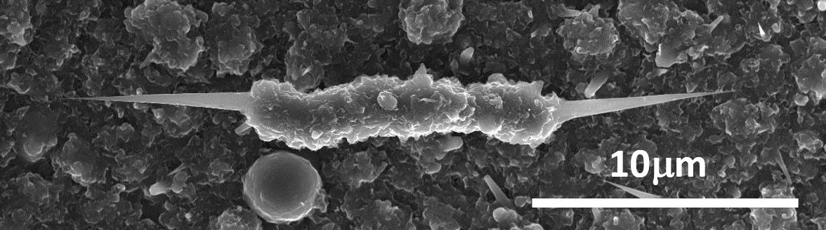
CnC exhibit an all-graphene-based morphology(1), made of a short microfiber segment with rough surface terminated at both ends by a sharp cone with smooth surface (Figure 1). They are prepared in a two-step CVD process(2), so that the nanocones form onto primarily-grown individual carbon nanotubes(3) (CNT).
CnC were successfully tested as electron emitters. They were mounted at the tip of a tungsten cathod of a cold-field emission gun (FEG) inside a dual-beam microscope FEI Helios NanoLab 600i. A micro-tip was used to move the carbon nanocone, and a focused ion beam to cut and to weld it(4). Good electrical conductivity of carbon nanocones was ascertained, along with the fact that these sources have a brightness 5 times greater than the sources marketed for TEM(5). However, CnC can be amorphized by the ion beam during the mounting preparation. Whereas this is not prohibitive for FEG sources, it is for other types of microscopy.
A new potential application of these carbon nanocones is their usage as SPM probes. There is a large variety of SPM modes (AFM, STM, KFM, etc.), each of them requiring probes with specific properties, e.g., sharpness, high aspect ratio, wear resistance, electrical conductivity. Most of the probes currently on the market are Si-based, while some others are based on carbon nanotubes or diamond. As they are made of perfect graphenes, CnC should produce probes with much higher quality than existing ones for several SPM modes.
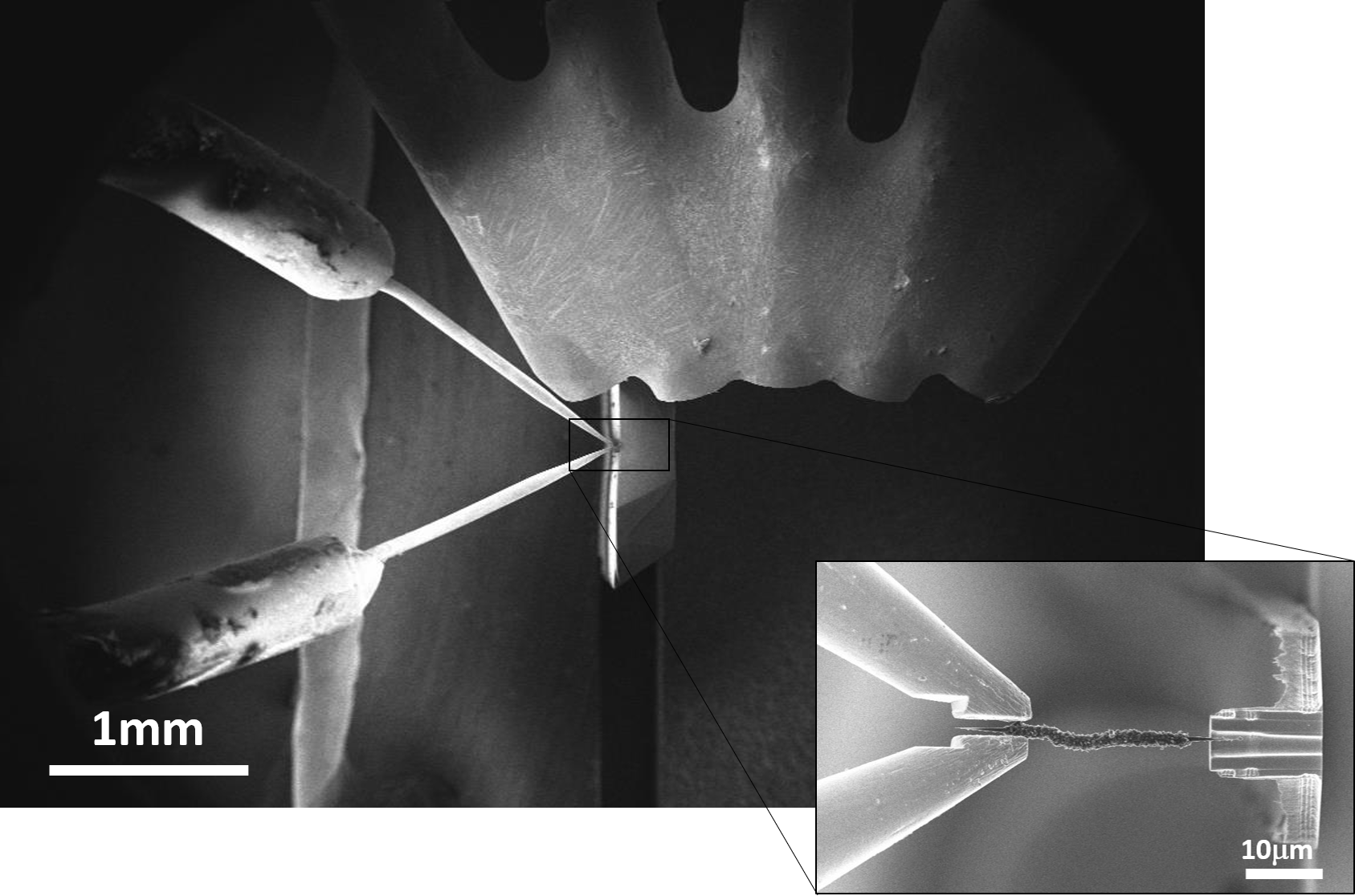
Two new mounting methods were investigated to avoid the irradiation of nanocones by the ion beam. The first technique consists of manipulating the nanocone with a micromanipulator under an optical microscope and then gluing it onto a cantilever-substrate with a UV-curing resin. The second technique uses welding with W by means of Focused Electron Induced Deposition (FEBID) in a Scanning Electron Microscope (SEM) equipped with micro-tweezers (Figure 2).
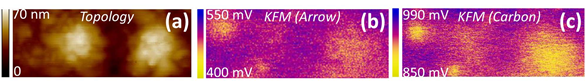
Carbon nanocones prepared as such were tested in different SPM modes and gave interesting and very promising results (Figure 3). They were found to exhibit similar, and sometimes better, performances than the reference probes regarding resolution, and much better performances regarding probe durability, with the additional interest that a same probe can be used for several modes (e.g., AFM, c-AFM, and KFM).
Our work is now focused on assessing the efficiency and reproducibility of the preparation procedures involving CnC, two fundamental aspects for pursuing the studies of these amazing objects.
Acknowledgments
The authors acknowledge the French National Research Agency under the "Investissement d'Avenir" program reference No. ANR-10-EQPX-38-01.
The LabEx NEXT is thanked for funding the "CarboProbe" project.
Figure 1. Overall morphology of a typical so-called "carbon nanocone".
Figure 2. Mounting of a carbon nanocone on an AFM cantilever.
Figure 3. (a) 3 µm wide topology image (AFM) of intermetallic particles in an aluminium alloy (A2024) surface. (b) KFM image (Arrow); (c) KFM image (carbon nanocone). Contrast in KFM mode reveals the work function differences (surface potential differences) with respect to the substrate (or the matrix, here Al).
- References
References
(1) Allouche, H., Monthioux, M. (2005). Chemical vapor deposition of pyrolytic carbon on carbon nanotubes. Part II: Texture and structure. Carbon 43, 1265-1278
(2) Jacobsen, R.L., Monthioux, M. (1997). Carbon beads with protruding spicules. Nature 385, 211-212
(3) Allouche, H., Monthioux, M., Jacobsen, R. (2003). Chemical vapor deposition of pyrolytic carbon on carbon nanotubes: (I) synthesis and morphology. Carbon 41, 2897-2912
(4) Houdellier, F., Masseboeuf, A., Monthioux, M., Hÿtch, M. J., “New carbon cone nanotip for use in a highly coherent cold field emission electron microscope”, Carbon 50, 2037-2044, 2012
(5) S. Mamishin, Y. Kubo, R. Cours, M. Monthioux and F. Houdellier, “200 keV cold field emission source using carbon cone nanotip: Application to scanning transmission electron microscopy,” Ultramicroscopy, vol. 182, pp. 303-307, 2017