Nano-scale Thermometry in 2-D Materials Using Low-Loss EELS
- Abstract number
- 686
- Event
- European Microscopy Congress 2020
- DOI
- 10.22443/rms.emc2020.686
- Corresponding Email
- [email protected]
- Session
- PST.4 - Spectroscopies in Electron, X-ray and Ion Microscopy
- Authors
- Professor Robert Klie (1), Dr. Xuan Hu (1), Mr. Bibash Sapkota (1), Professor Serdar Ogut (1)
- Affiliations
-
1. University of Illinois at Chicago
- Keywords
2-D Materials, EELS, in-situ, STEM
- Abstract text
Two-dimensional materials, including graphene, BN and transition metal dichalcogenides (TMDs), exhibit great potential for a variety of applications, such as transistors, spintronics, or photovoltaics. [1-2] When 2-dim materials are used in electronic devices, the potential for miniaturization offers remarkable improvements in electrical performance. Yet, controlling the heat flow across a hetero-structure will be crucial to developing high-speed electronic devices based on 2-dim materials. We have recently shown that the thermal expansion coefficient (TEC) dramatically increases in 2-dim materials when the thickness of the material shrinks from bulk to a few monolayers.[3] Therefore, the TEC mismatch of 2-dim materials becomes an additional concern in designing electronic nano-devices. More specifically, we need to develop methods that enable us to control and tailor the TEC of TMDs through alloying or defect engineering.
In this contribution, we will utilize atomic-resolution imaging and electron spectroscopy in an aberration-corrected scanning transmission electron microscope (STEM) to characterize the thermal properties of 2D materials, including pristine and allowed transition-metal dichalcogenides. Specifically, we will use the aberration-corrected JEOL ARM200CF at the University of Illinois at Chicago, equipped with a cold-field emission electron source and a Gatan Continuum GIF. Specifically, we will measure the thermal expansion coefficient of monolayer Mo1-xWxS2 materials with 0 ≤ x ≤ 1 using our plasmon-EELS based approach.[3] Various 2D materials are heated up to 700 K in our ProtoChips Aduro double-tilt stage and high-resolution imaging and EEL spectroscopy are performed on single layer particles. The experimental data is then compared to our first-principles modeling results, based on special quasi-random structures, as well as structures directly extracted from the high-angle annular dark-field (HAADF) images of alloyed TMDs. In-situ heating experiments will also be conducted to test the effects of temperature and strain on phase separation in alloyed TMDs.
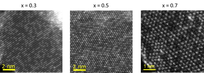
Figure 1 show several HAADF images of Mo1-xWxS2, where the heavier W atoms can be clearly identified as the brighter image contrast. The shift of the plasmon peak is then measured as a function of temperature in these materials, while the corresponding shift as a function of lattice parameter is calculated using DFT calculations in the random phase approximation (RPA). Combining the experimental and modeling data, we can now predict the TEC for the Mo1-xWxS2 alloys, as show in Figure 2. It is interesting to note here that the thermal expansion coefficient appears to be largest in the Mo0.5W0.5S2 samples and appears independent of the structural model used.[4]
Figure 1. Atomic-resolution images of monolayer Mo1-xWxS2 at 300 K.
Figure 2. Special quasi-random structure a) top view and b) side view used to calculate the thermal expansion coefficient in Mo1-xWxS2 below 700 K.
We will also explore the thermal stability and thermal expansion behavior of other TMD alloys, such as Mo1-xVxS2. First-principles modeling suggests that the formation of an alloy requires moderate synthesis temperatures. The phase stability, structural stability as well as the atomic structure of 2-d particles edges in Mo1-xVxS2 will be explored during in-situ heating experiments and compared to our DFT models. These results will lead to more accurate model for predicting stable TMD alloy structure with novel electronic and electro-chemical properties.[5]
- References
[1] B. Standley et al., Nano Lett., 8 (2008), p. 3345–3349.
[2] W. Han et al., Nature Nano, 9 (2014), p. 794–807.
[3] X. Hu et al., Phys. Rev. Lett., 120 (2018), p. 055902
[4] X. Hu et al., Small, 16(3), p. 1905892 (2019)
[5] This work was supported by the National Science Foundation (DMREF CBET-1729420)