Nanoplate’s crystallography: A full description using pseudo-kinematical electron diffraction
- Abstract number
- 669
- Event
- Virtual Early Career European Microscopy Congress 2020
- Presentation Form
- Submitted Poster
- DOI
- 10.22443/rms.emc2020.669
- Corresponding Email
- [email protected]
- Session
- PSA.5 - Nanoparticles & Catalysts
- Authors
- Ms Miriam Carolina Mendoza-Ramirez (1), Professor Miguel Avalos-Borja (1)
- Affiliations
-
1. Instituto Potosino de Investigación Científica y Tecnológica A. C.
- Keywords
Diffraction
Hexagonal Au
Precession
- Abstract text
Summary
Discussion on plate nanoparticle´s (NP) forbidden reflections (FR) have prevailed for at least 40 years, [1] partly due to the “dynamical effects” present on Selected Area Electron Diffraction (SAED) has hindered NP´s fine structure determination. On this work the use of Precession Electron Diffraction technique (PED) [2] have had a pivotal role on describing novel aspects of these particles complementing and extending the understanding of Au triangular nanoparticles structure.
Introduction
Au nanoplates have several applications on different fields as Surface-Enhanced Raman Spectroscopy (SERS), photovoltaics, molecular detection or photothermal cancer therapies. Plate’s properties can be determined by either, size, shape or structural defects. The last property is typically characterized by SAED, due to nanoparticles characteristics dimensions.[3] However, this technique is often affected by the dynamic diffraction effect, producing FR and giving useless (for fine structure determination) ED patterns in most cases.
Nanoplates have been distinguished due to the 1/3{422} FR which have been “explained” by several models, such as stacking faults, [4] twins or thickness effects. [5][6] Unfortunately these models have not been verified, mainly because there are no experiments with the ability to study these particles three-dimensionally.
On this work, recent advances on the full nanoplate’s crystallographic description are presented. Relevant highlights from this research are that Au nanoplates were three-dimensionally studied in two aspects, morphology (front and side view) and structure. Several improvements on nanoplate’s characterization were obtained by using the PED technique and the tridimensional cell parameters for a novel hexagonal Au unit cell (Auhex) will be presented. The lattice parameters for this phase were determined using kinematical experimental data. Additionally, this work discusses and dismisses those models which are inconsistent with our experimental results. A model considering “two phases” is proposed and corroborated by using kinematical simulation. According to this model it was found that there are two phases involved (Aufcc and Auhex), which keep specific crystallographic orientation relationships.
Materials and methods
Nanoplate’s syntheses procedure: Au NP´s were synthetized according to a well-known published polyol process. [7]
TEM characterizations: TEM samples were prepared by diluting samples in isopropyl alcohol and mounted on Cu grids. Bright field (BF) Characterizations were achieved using a FEI Tecnai-F30 TEM at 300 kV. NP were oriented by using a double tilt sample holder. For PED acquisition a Spinning Star P-20® PED unit was used, with a precession angle of 2.4°. Micrographs were acquired by using a Gatan® Orius SC200 digital camera. Digital Micrograph® and Mac Tempas® software were used for micrograph treatment and kinematical diffraction simulation, respectively.
Results and Discussion
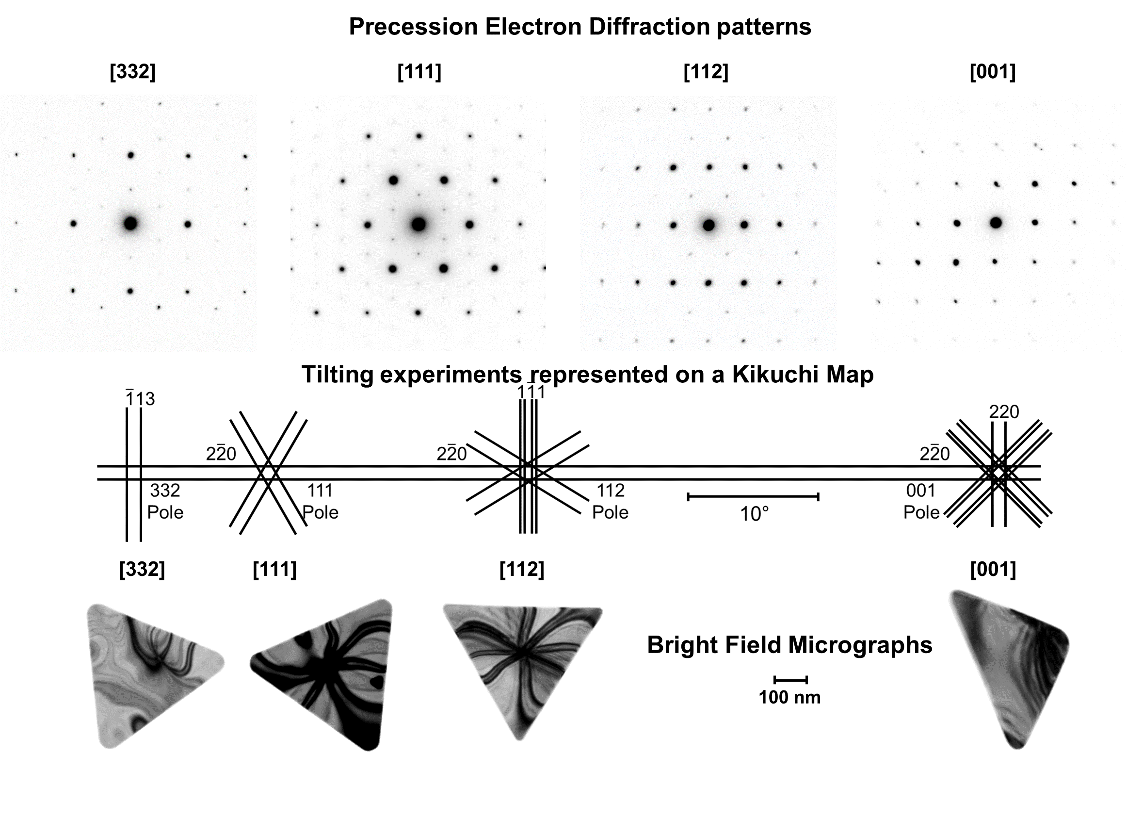
Polyol synthesis produces a great variety of products (rods, wires, decahedrons, tetrahedrons, etc.). However, this study was focused only on triangular plates like those shown on Figure 1.
For acquiring information on the particle´s three dimensions several tilting experiments like those shown on Figure 1 were done. Nanoplates in this figure exhibit diffraction contrast as bending contours in image mode. This contrast can be directly related with nanoparticle´s orientation. As can be seen in Figure 1, this experiments were obtained tilting around the [1-10] direction, covering an angular space of more than 60 degrees. Nevertheless, for several experiments it was also possible to acquire nanoplate´s Zone Axis Patterns (ZAP) on side view, making plate’s three dimensional characterization possible.
In terms of diffraction, the PED technique enables to obtain patterns that look perfectly oriented and with minimized dynamical diffraction effects (intensity profiles will be properly discussed on poster presentation). Patterns presented on this abstract were indexed according to a cubic FCC phase, but in all of them it is possible to note FR´s as can be observed in the patterns of Figures 1 and 2.
Figure 1. Typical experiments on which nanoplates were tilted away from [111] zone axis.
By studying symmetry and spot position in all obtained patterns, several assertions were proposed. The first observation is that 1/3{422} FR are not really produced by double diffraction, otherwise, their intensity would have been dramatically minimized by the use of the PED technique, therefore these spots are most likely produced by stacked fault planes and are not forbidden by space group symmetry. The second proposed statement, implies the existence of two diffracting lattices. One is a perfect cubic crystal and the second is a hexagonal crystal whose lattice parameters were measured directly on ZAP+ PED patterns.
For describing experimental results a model which included two gold phases was besought. The first phase in this model is the well-known Au structure, exhibiting strong diffraction spots and the second one is a hexagonal structure which has a weaker intensity due to the fact that diffracted spots arise from only a few atomic layers.
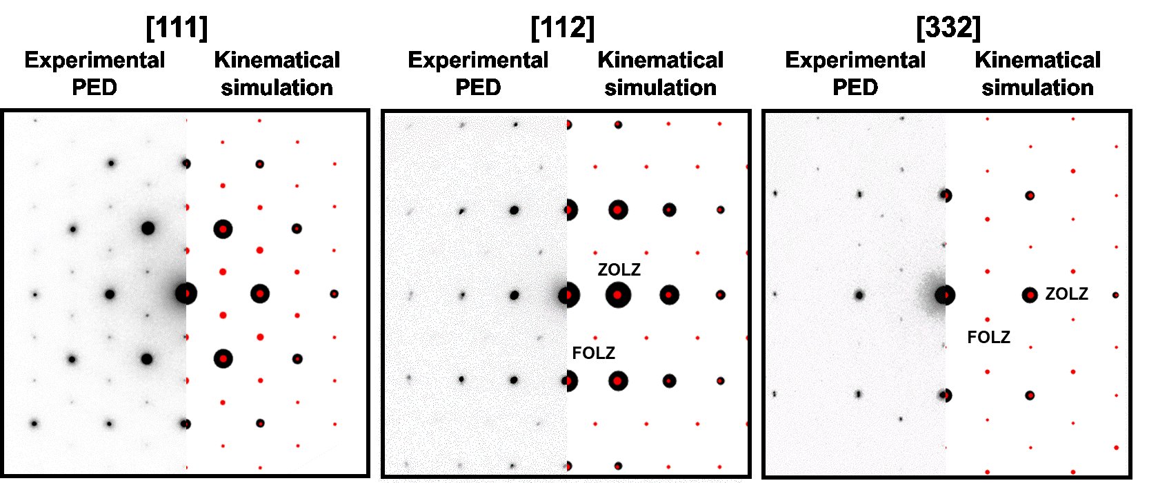
Figure 2. Kinematical simulations are shown for three experimental patterns.
To verify experimental results (as those in Fig. 2) we simulated kinematical diffraction patterns assuming for Aufcc the typical No. 225 space group and for Auhex the hexagonal No. 174 space group structure. For these two phases a specific orientation relationship was fixed. For several directions, the hexagonal phase was so thin that ZOLZ and FOLZ could be found on simulation, reproducing all experimental patterns.
Conclusion
PED characterizations prove to have better precision than those performed using SAED for characterizing nanoplates. A “two phase model” was able to reproduce experimental patterns on more than eight different zone axis diffraction patterns in TNP.[8]
- References
[1] K. Heinemann, et al., J. Cryst. Growth, 47(2),177–186, 1979.
[2] R.Vincent. and P.A.Midgley, Ultramicroscopy, 53 (3), 271–282, 1994.
[3] J. E. Millstone, et al., Small, 5(6), 646–664, 2009.
[4] V. Germain, et al., J. Phys. Chem. B, 107(34), 8717–8720, 2003.
[5] A. I. Kirkland, et al., R. Soc., 440, 589–609, 1993.
[6] J. Reyes-Gasga, et al., Ultramicroscopy, 108 (9), 929–936, 2008.
[7] C. Kan et al., J. Nanomater., 2010, 1–9, 2010.
[8] We thank the LINAN laboratories, Hector Silva-Pereyra and Lucia Aldana-Navarro.