Nanosatellite and void formation in Ion Irradiated SiOx and SiNy studied via TEM
- Abstract number
- 1397
- Event
- European Microscopy Congress 2020
- DOI
- 10.22443/rms.emc2020.1397
- Corresponding Email
- [email protected]
- Session
- PSA.3 - Semiconductors & Devices
- Authors
- Dr P. Mota-Santiago (3), Dr. Felipe Kremer (1), Prof. G. Rizza (4), Prof. C. Dufour (2), Dr. C. Notthoff (3), A/Prof. P. Kluth (3)
- Affiliations
-
1. Centre for Advanced Microscopy, The Australian National University, 131 Garran Road, Acton 2601
2. CIMAP/ENSICAEN, 6 Boulevard Maréchal Juin
3. Department of Electronic Materials Engineering, Research School of Physics, Australian National University, Acton 2601
4. Laboratoire des Solides Irradiés (LSI), Ecole Polytechnique, UMR 7642 CEA, DSM, IRAMIS, CNRS
- Keywords
Swift heavy ion irradiation, HAADF, Nanosatellites
- Abstract text
A phenomenon observed in addition to the ion-shaping process during swift heavy ion irradiation (SHII) is the formation of small nanoclusters surrounding the irradiated NPs when embedded in a-SiO2 [1]. As the NPs begin to elongate with increasing fluence, the energy deposited by the ion increases concomitantly, likewise the energy per atom increases near the boundary and can surpass the energy required for vaporization. This can lead to the dissolution of Au atoms into the matrix which are likely to aggregate into small nano-clusters due to the low solubility and reactivity.
To study and formation of nanosatellites (NSs) and voids, a combination of plasma enhanced chemical vapour deposition and metal sputtering was utilized to obtain the SiOx/Au/SiOx/Si(001) and SiNy/Au/SiNy/Si(001) heterostructures. Post deposition ion irradiation with 185 MeV Au+ ions with fluences ranging from 1.0×10¹² to 1.0×10¹⁴ at·cm-2 was then carried out to form the elongated Au NPs embedded in SiO1.9 and SiN1.06.
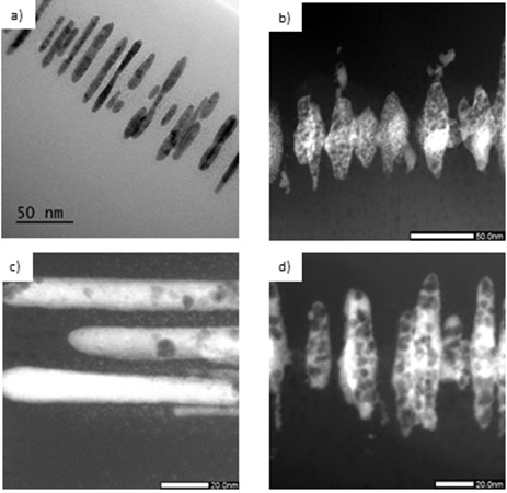
Figure 1(a) displays elongated Au NPs in a-SiO1.9 after irradiation to a fluence of 1×1014 cm-2. In the image, the formation small NSs between the elongated NPs is evident. Figure 1(b) shows the Au NPs embedded in a-SiN1.06 under the same irradiation conditions. No evidence of NS formation was found; however, the formation of cavities is clearly visible inside the Au particles and in the SiN1.06 substrate. Due to its high mass contrast, HAADF was utilized to inspect for the formation of small NSs otherwise hard to distinguish in conventional TEM. For the SiO1.9 case [Fig. 1 (c)] we can observe in more detail the distribution of the NSs around the elongated NPs. It appears that each elongated NP possess a halo of NSs which are within 10 nm from the NPs surface. For the SiN1.06 case [Fig. 1 (d)], a different behaviour is observed, where no clear presence of NSs can be detected.
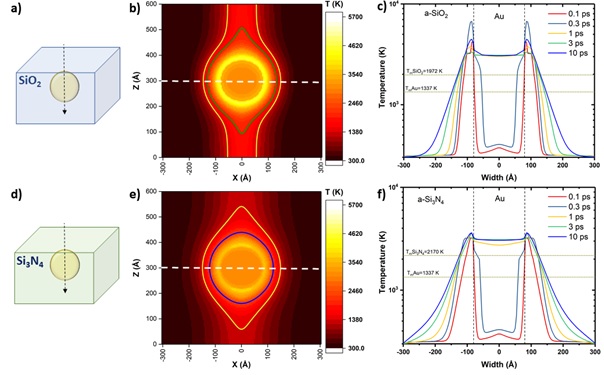
A possible pathway for the formation of NSs in a-SiO1.9 and not in a-SiN1.06 can be explained based on the thermal profile during the ion shaping process. From the plots shown in Figure 2 (c) and (f) the temperature profile inside the Au NP can be observed to follow a similar trend and appears to reach the same temperature (≈3100 K) when embedded in a-SiO2 and a-Si3N4 yet, when embedded in a-SiO2, the formation of a shell of nearly 2 nm thickness inside the NP is observed between 3 and 10 ps that reaches temperatures of ≈3500 K. Such localised increment in temperature might be a consequence of the lower thermal conductivity of a-SiO2 that prevents the heat flow to the matrix as efficiently as in a-Si3N4. Therefore, one possible condition is the necessity of surpassing the boiling temperature of Au (3129 K) to form NSs, a condition not reached when embedded in a-Si3N4 due to the high thermal conductivity of the substrate.
Besides reaching a high temperature at the metal/dielectric interface, the Au atoms require a medium where they can diffuse outwards from the NP. It is well-known from ion implantation experiments that Au atoms exhibit high mobility in a-SiO2. Results, however, have not been reported for a-Si3N4, but it is known as a material exhibiting low diffusion coefficients for a broad range of impurities. Because the region surrounding the NP exceeds the melting point of a-SiO2 [see Fig. 2 (c)] a high mobility of Au monomers is expected that can extend several nanometres from the surface of the NP. A different behaviour can be expected in a-Si3N4. Despite showing a region above the melting point of Au extending about 10 nm at t = 10 ps, the combination of a low diffusion coefficient and lower temperature compared to a-SiO2 can prevent the increase of Au monomer density around the elongated NP. For example, while the presence of very small clusters (sizes < 1 nm) cannot be ruled out due to the resolution, the micrographs show no cluster formation in a-SiN1.06, whereas in a-SiO1.9 they are clearly visible. On the other hand, the low solubility of Au in a-SiO2 and the favourable conditions for the monomer production during the ion-shaping process, facilitate the formation of NSs. This agrees with the observation of a higher nano-satellite density in SiO1.9 [Fig. 1 (c)] but not for a-SiN1.06 [Fig. 1 (d)].
In addition to NSs, the micrographs shown in Figure 1(c) and (d) show that the elongated Au NPs in a-SiO1.9 and a-SiN1.06 contain cavities leading to nano-porous metal structures. During annealing to temperatures near the melting point, a-Si3N4 is known to decompose into a-Si and N2 [2]. While the nature of the cavities has not been identified in a-SiN1.06 [Fig. 1(b)], i.e. if they are gas-filled or empty voids, it is possible they penetrate the Au NP at the Au/a-SiN1.06 interface during the SHII process leading to the observed porous NPs.
In summary, the evolution of Au metal nanoparticles submitted to SHII leading to the formation of NSs and Au cavities can be explained under the framework of the 3D i-TS model [3] and the different thermal properties of SiO2 and Si3N4.
Figure 1. TEM BF (a) and (b), and HAADF in STEM mode (c) (d) images of Au NPs embedded in a-SiO1.9 [(a) and (c)], and a-SiN1.06 [(b) and (d)] after irradiation with 1×1014 cm-2.
Figure 2.Configuration of the 3D-iTS calculation cell and snapshots of the three-dimensional thermal evolution of a Au NP of 16 nm in diameter while embedded in a-SiO1.9 [(a) and (b)] or a-SiN1.06 [(d) and (e)] after 10 ps. Solid lines were added to show the region surpassing the melting point of a-SiO1.9 (green), a-SiN1.06 (dark blue) and Au (dark yellow). Temperature profile along the transversal direction (white dotted lines) at different times for a-SiO1.9 (c) and a-SiN1.06 (f).
- References
[1] Ridgway, M. C., et al. 9, 2011, Physical Review Letters, Vol. 106.
[2] Haddad, T. M. Advanced Multilayered and Fibre-Reinforced Composites. Netherlands : Springer Netherlands, 2012.
[3] Dufour, Ch, et al. 2012, J. Phys. D: Appl. Phys., Vol. 45, p. 065302.