Nanoscale observations of dynamical processes in layered Ge–Sb–Te based alloys and heterostructures
- Abstract number
- 417
- Event
- European Microscopy Congress 2020
- DOI
- 10.22443/rms.emc2020.417
- Corresponding Email
- [email protected]
- Session
- PSA.2 - Metals & Alloys
- Authors
- Andriy Lotnyk (2), Torben Dankwort (1), Isom Hilmi (2), Lorenz Kienle (1), Bernd Rauschenbach (2)
- Affiliations
-
1. Institute for Materials Science, Faculty of Engineering, University of Kiel
2. Leibniz Institute of Surface Engineering (IOM)
- Keywords
phase change memory alloys, heterostructures, superlattices, phase transitions, in situ microscopy
- Abstract text
Summary
This work reports a direct, nanoscale observations of the order-disorder processes in layered Ge-Sb-Te based thin films heterostructures using in situ experiments inside an aberration-corrected scanning transmission electron microscope. The findings reveal reversible self-assembled reconfiguration of structural order in those layered materials. The process is associated with ordering of randomly distributed vacancies within of the studied alloys into ordered vacancy layers and with readjustment of lattice plane distances within the newly formed layered structures, showing high flexibility of the layered chalcogenide-based systems. Overall, the outcomes provide new insights into local structure and switching mechanism in chalcogenide superlattices
Introduction
Ge-Sb-Te-based alloys are employed in data storage and memory technology whereas layered GeTe–Sb2Te3-based superlattices (SLs) are considered to be a main contender for memory devices with low power consumption. The reduction of switching energy is due to the lowering of entropic losses governed by the restricted motion of atoms in one dimension within the crystalline states. Elucidation of switching mechanisms in GeTe-Sb2Te3 SLs have recently attracted much attention. However, the proposed theoretical models are still under debate [1]. This is due to the lack of direct observation of atomic scale processes that might occur in those SLs. To close this gap, we apply in situ aberration-corrected atomic-resolution scanning TEM (Cs-corrected HRSTEM) for nanoscale observations of dynamical processes in GeTe-Sb2Te3 based SLs and in layered Ge-Sb-Te (GST) thin films [2]. The layered GST alloys resembles a model structure for the investigations of the material properties of the SLs.
Methods/Materials
Epitaxial GeTe-Sb2Te3 based SLs and layered trigonal GST-based thin films grown by pulsed laser deposition (PLD) were used for in situ TEM experiments. The in situ observations were done by using a TEM heating holder and a focused electron beam as a tool for in situ manipulation of atomic species in the crystal lattices.
Results and Discussion
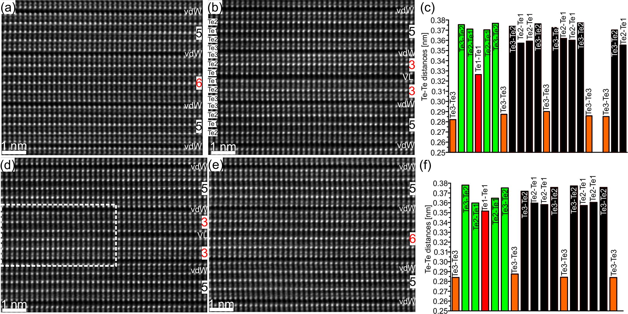
The as-prepared trigonal GST thin film exhibited local chemical disorder, which is associated with the formation of GST structural units with 5 and 6 Te layers per unit (Figure 1(a)). In situ heating of TEM specimen to a TEM holder temperature of 240 °C resulted in a change of the structural order of the GST thin film (Figure 1(b)). The GST building units with 5Te layers did not change much at this temperature. On the other hand, the building blocks with 6Te layers decomposed into two GST blocks with 3 Te layers per unit. These blocks with 3 Te layers were stable up to a temperature of 320 °C and remained in the TEM specimen after cooling down the specimen to a room temperature (Figure 1(b)). The empty space between the blocks with 3 Te layers in Fig. 1(b) is a vacancy layer. The vacancy layers (VLs) and van der Waals like gaps (vdW) in GST materials can be distinguished by an increased atomic distance between two adjacent Te-Te layers for the VLs. Analysis of distances between Te-Te planes across the VL revealed slightly larger values compared to the distances across the vdW gaps (Figure 1(c)). However, the reduction of Te-Te distances into the VL does not influence the Te-Te distances next to the vdW gaps of the whole layered structure. The relaxation of Te into VL led indeed to readjustment of Te-Te distances within the 3 Te layered structures. As a result, the Te-Te distances close to the VL in such structures are expanding and becoming nearly equal while the distribution of distances between Te-Te planes in the preceded 6-fold layered units are not uniform.
Electron beam exposure of newly formed 3-fold Te layered structures resulted in the filling of VLs by Ge and Sb atomic species. Consequently, a recovery back into the initial 6 Te layered structure is observed (Figure 1(d)-(f)). The reconfiguration of GST building blocks leads to expanding distances between Te-Te planes next to the VL, thus almost resembling the distances of initial structure and the relaxation of the whole layered system (Figure 1(f)). In addition, the 3 Te layered structures can be artificially produced by local heating of recovered Ge/Sb layers using a focused electron beam [2]. Thus, the formation and recovery of VL within of 6 Te layered building blocks is identified as a reversible process.
Similar results were observed after the in situ experiments using GeTe-Sb2Te3 SLs [2].
Figure 1. Atomic-resolution HAADF-STEM images of (a) initial GST layered structure before in situ TEM heating and (b) after in situ TEM heating to a temperature of 320 °C. (c) Te-Te distances within and between the 3 Te and 5Te layered structures. The Te-Te distances on the right part (three bars only) are calculated distances extracted from a simulated image containing a 5 Te structure. (d) Partial filling of VL after electron beam exposure of the specimen area marked by dashed rectangle. (e) Complete filling of VL after electron beam exposure of image (d). (f) Te-Te distances after complete transformation of 3-fold Te layered structure to 6-fold Te structure. The numbers in HAADF micrographs give the quantity of Te layers per building unit.
Conclusion
Nanoscale processes in layered Ge-Sb-Te thin films and GeTe-Sb2Te3 based SLs were investigated by different in situ TEM methods. Based on the experimental observations, a possible switching mechanism in chalcogenide-based SLs can be proposed. The mechanism supposes two processes running simultaneously upon switching of the SLs. The first process supposes reconfiguration of (GeSb)Te layers at the vdW interfaces between GST and Sb2Te3 building units, whereas the second process includes an order-disorder process in thick Ge-Sb-Te layered structures.
- References
[1] X.-B. Li, N.-K. Chen, X.-P. Wang, H.-B. Sun, Adv. Funct. Mater. 28 (2018) 1803380
[2] A. Lotnyk, T. Dankwort et al., Nanoscale 11 (2019) 10838-10845