Observation of chemical-vapor-transport-based processes utilizing µReactor
- Abstract number
- 326
- Event
- European Microscopy Congress 2020
- DOI
- 10.22443/rms.emc2020.326
- Corresponding Email
- [email protected]
- Session
- PST.6 - In-situ and in-operando microscopy
- Authors
- Libor Novák (4), Kristýna Bukvišová (1), Zhu-Jun Wang (2), Vojtěch Mahel (4), Marc Georg Willinger (2), Tomáš Šikola (3, 1), Miroslav Kolíbal (3, 1)
- Affiliations
-
1. Ceitec BUT
2. ETH
3. Institute of Physical Engineering, Brno University of Technology
4. Thermo Fisher Scienetific
- Keywords
in-situ SEM, MicroReactor, graphene, nanowires, 2D materials
- Abstract text
Summary
Chemical-vapor-transport reactions were maintained and in-situ imaged in SEM using a µReactor device.
Introduction
1D and 2D materials are new classes of nanoscale materials attracting a lot of attention in recent years. A full understanding of their growth and modification process necessitates the use of real-time in-situ microscopy, which is practically the only technique capable of delivering quantitative assessment of the mechanisms involved in the growth. The difficulty in gaining such a predictive power is mostly related to a very high spatial resolution, which needs to be maintained even in very harsh conditions related to the growth: high temperature and pressure. Here, we present an approach for in-situ SEM imaging of chemical-vapor-deposition (CVD) and transport, demonstrated on graphene and other relevant material systems.
Methods
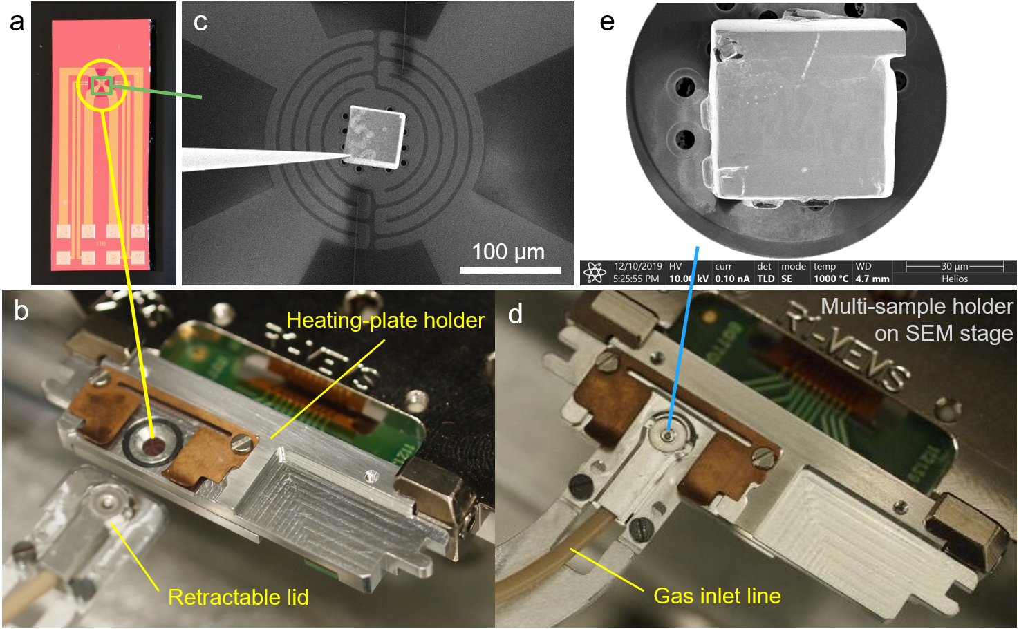
In order to image nanoscale processes at very high resolution, we have designed a µReactor device [1], which allows for gas injection into a small differentially pumped volume surrounding the processed sample. Sample heating is assured by a micro-heating plate. Compared to the environment of the whole SEM chamber, the smaller volume of the reactor separated from the SEM chamber by pressure limiting aperture assures higher cleanliness of the processes. The initial sample or a reaction substrate is prepared on the heater, typically by FIB lift-out from bulk in a FIB/SEM system. The reaction volume is closed by a retractable lid without the need for venting of the SEM chamber (Fig. 1). Aperture in the lid allows direct SEM imaging of the heat & gas stimulated process on the sample and at the same time it can keep the reactor space at overpressure of several hundred of pascals. SEM is operated in high vacuum mode with SEM chamber pressure < 1E-2 Pa. Standard SEM detection including in-lens is thus possible. The temperature of the heating plate is calculated from heating wire resistance [2]. Pressure in the reaction volume is estimated from heater temperature and heating power based on the Pirani gauge principle. Another advantage of the used approach is that pressure up to 500 Pa inside the reactor can be achieved using relatively low inlet flow rates (units of sccm) of a (reactive) gas, which can then easily be mixed with inert gases in the SEM pumping system to reach safe concentration at the outlet. The gas feeding system is built outside the microscope and allows mixing of different gas lines and their precise control by mass flow controllers and/or leak valves before entering the inlet capillary of the reactor. The small volume of the reactor space thus allows to safely use different gases and their mixtures (including hydrogen and ethylene for graphene growth).
Results and Discussion
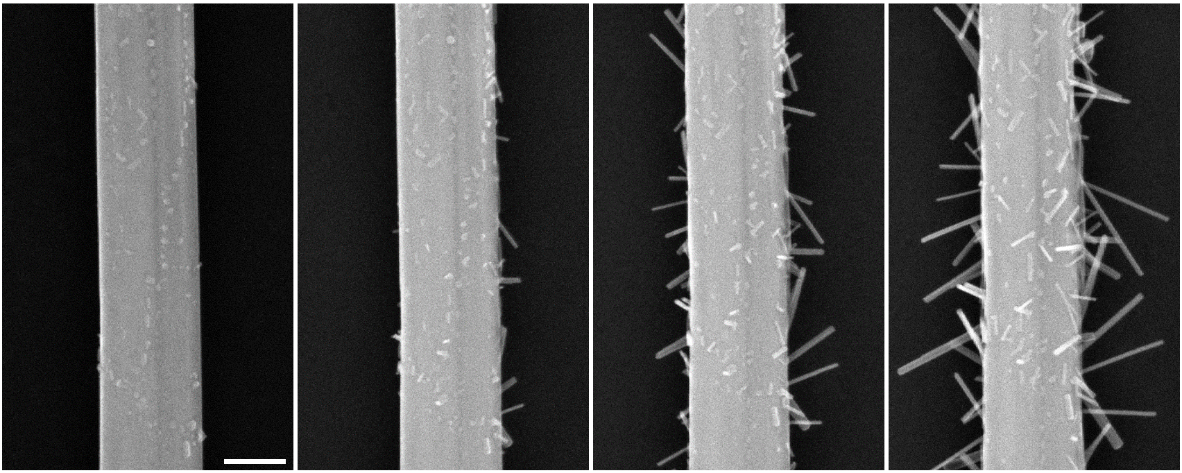
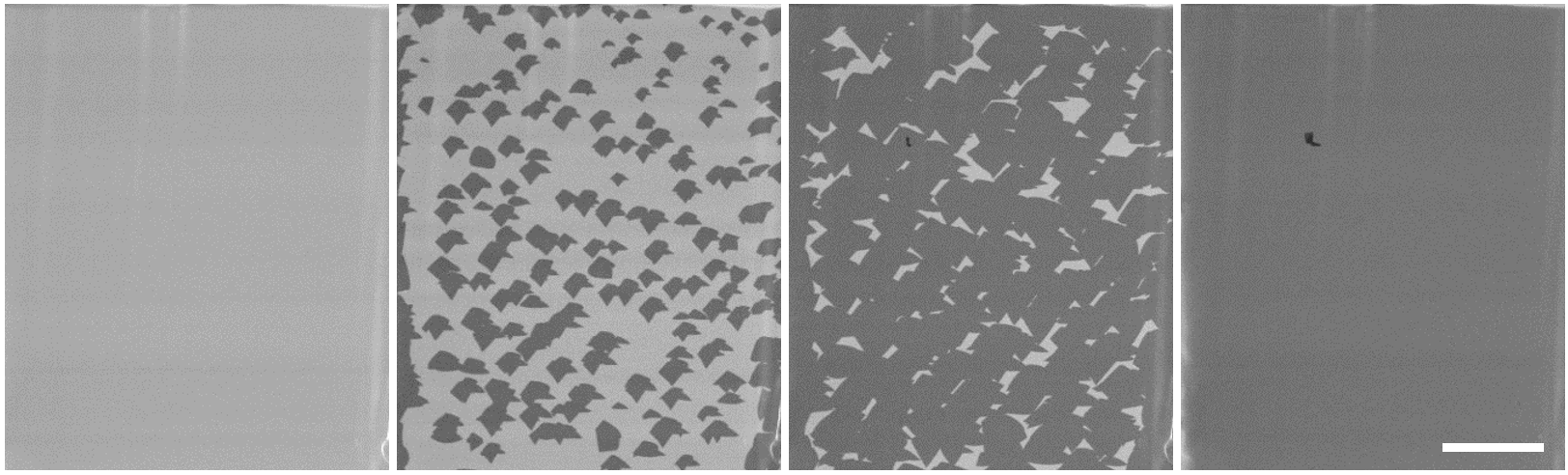
As the first proof-of-concept experiment, we will show an oxidation reaction of tungsten disulfide nanotubes and platelets in a water vapor (up to 10 Pa) at elevated temperature (450-600°C). The oxidation process results in formation of tungsten oxide nanowires (Fig. 2) and continues until the whole nanotube gets consumed. The real-time imaging allows to track the kinetics of the process and together with additional characterization techniques allows to quantitatively describe the oxidation mechanism [3]. In another experiment, we have used a small chunk (tens of micrometers wide) cut out from a polycrystalline platinum foil (25 microns thick) by FIB in Helios FIB-SEM, which was glued to the heating plate in the µReactor by tungsten deposition. In the first step of this in-situ SEM experiment, the sample was heated to temperatures between 900°C and 1000°C and cleaned in the flow of pure hydrogen (30 Pa to 50 Pa H2 pressure in the sample area). This procedure leaves very clean platinum surface with minimal amount of carbon residuals (left image of Fig. 3), which is essential for graphene formation [4]. Ethylene was introduced in the second step of the experiment together with continuous hydrogen flow. Formation of graphene islands with the expected characteristic shape [5] [6] was observed in the initial phase of the growth (Fig. 3). Growth of graphene monolayers [7] was controlled by partial pressure of ethylene (adjusted in the range of 5 Pa and 10 Pa) and by sample temperature (between 900°C and 1000°C).
Conclusion
The proof-of-concept experiments we have made so far demonstrate the versatility of the µReactor concept and the advantages it offers if compared to a more common reactive gas dosing into the whole microscope chamber. We have just started to uncover the full potential of the µReactor and we will present our latest results on other material systems as well.
Figure 1: µReactor with a micro-heating plate (a). In open state (b), a piece of bulk sample can be placed on the heater using FIB lift-out and transfer on EasyLift needle (c). Reaction volume is closed in next step by a retractable lid (d). Aperture in the lid (in blue) assures overpressure (up to 500 Pa) in sample area, while the SEM chamber remains at high vacuum. When used on Helios FIB/SEM system, high resolution in-situ SEM imaging during a heat & gas stimulated process is possible using in-lens TLD detector (e).
Figure 2: A series of SEM micrographs showing a WS2 nanotube (time span between images: 3 minutes) oxidized in 10 Pa water vapour at temperatures 500-570°C. The experiment allowed for direct analysis of temperature-dependent reaction kinetics. Scale bar length is 100 nm.
Figure 3: Graphene growth on platinum substrate imaged in-situ in the µReactor using TLD-SE detector in UHR mode of Helios UC. Formation of graphene on clean platinum surface was stimulated by sample temperature of 900°C and by hydrogen-ethylene environment (5 Pa C2H4 and 30 Pa H2). Image sequence was acquired over 45 seconds. Scale bar length is 10 µm.
- References
[1] L Novak, M Kolibal, M Wu, P Wandrol, T Vystavel, Microscopy and Microanalysis, 24(S1) (2018), p. 808-809. doi:10.1017/S1431927618004531
[2] L Mele et al. , Microscopy Research and Technique 79 (2016) p. 239 https://doi.org/10.1002/jemt.22623
[3] M Kolibal, K Bukvisova, L Kachtik, A Zak, L Novák, T Sikola The Journal of Physical Chemistry C 123 (14), (2019) p. 9552-9559. doi: 10.1021/acs.jpcc.9b00592
[4] Z Wang, J Dong, Y Cui, et al., Nat Commun 7, 13256 (2016). https://doi.org/10.1038/ncomms13256
[5] Z Wang, J Dong, L Li, et al. ACS Nano 2020 just accepted. https://doi.org/10.1021/acsnano.9b08221
[6] Z Wang, G Weinberg, Q Zhang, et al., ACS Nano 2015, 9 (2), 1506-1519. https://doi.org/10.1021/nn5059826
[7] https://www.youtube.com/watch?v=GmIfGMcTsn0&list=PLhJ74CQiOr7bGhmkU2zOKMP-XXOhnLhOB