Off-axis holography of polarization fields under strongly diffracting conditions
- Abstract number
- 988
- Event
- European Microscopy Congress 2020
- DOI
- 10.22443/rms.emc2020.988
- Corresponding Email
- [email protected]
- Session
- PSA.3 - Semiconductors & Devices
- Authors
- Tore Niermann (1), Michael Lehmann (1)
- Affiliations
-
1. Technische Universität Berlin
- Keywords
Group III-Nitrides, Multislice calculations, Off-axis holography, Polarization fields
- Abstract text
Group III-Nitrides are a common semiconductor materials for electronic and optoelectronic devices. However, the spontaneous and piezoelectric polarization properties of these materials often have detrimental influence on the device efficiencies. Changes of the polarization as found at heterointerfaces lead for instance to reductions of recombination rates and red-shift of the emission lines, an effect also known as the quantum confined Stark effect [1].
Due to its high sensitivity to long-range changes of the electrostatic potential off-axis electron holography is one possibility to directly measure the occurring electrical fields directly with spatial resolution in the nanometer range [2]. Potential measurements are usually carried out under kinematic scattering conditions to avoid dynamical diffraction effects on the measured electron phase.
However, typical quantum well in InGaN/GaN laser devices have widths around 2 nm and extend in the (0002) plane. In a 200 nm thick specimen a tilt of 10 mrad away from on-edge orientation already leads to a broadening of interfaces of 2 nm, thus is already to large to allow the investigation of such thin quantum wells. This makes kinematic conditions unsuitable for the observation of these quantum wells, since these require the specimen to be tilted by far larger angles (for comparison the diffraction angle of (0002) beams at 300keV is at 7.7 mrad).
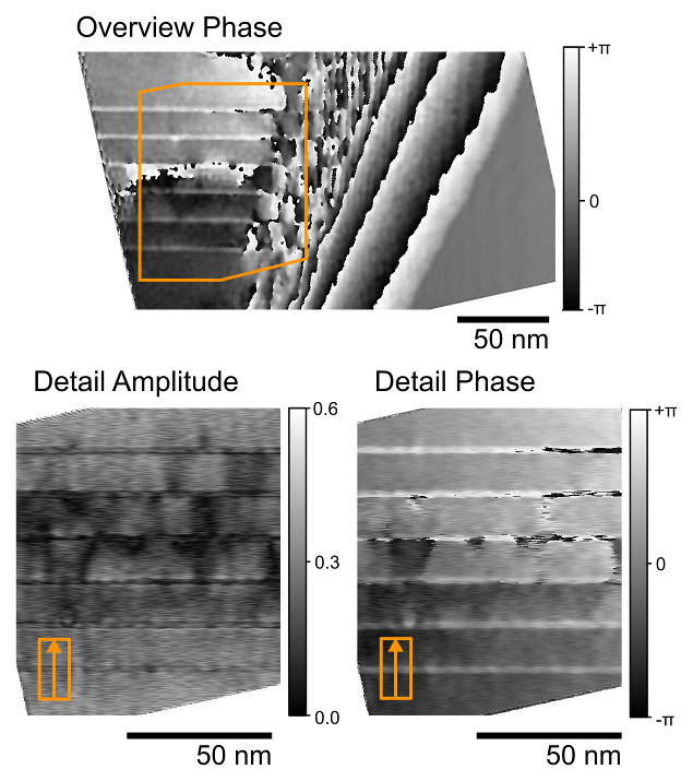
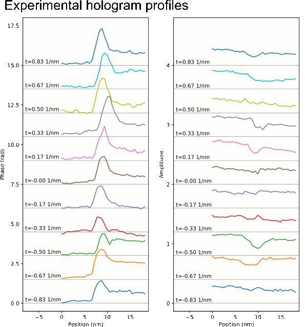
We recorded off-axis electron holograms of multiple 2.2 nm wide In0.15Ga0.85N-quantum wells embedded in a GaN matrix under (0002) systematic row conditions. We additionally varied the beam tilt along the systematic row in order to observe how dynamical diffraction effects alter the results. In Figure 1 the reconstructions of an overview and detail hologram of the 220+/-10 nm thick specimen are shown. The holograms are reconstructed with an anisotropic mask in order to preserve most of the high-resolution information perpendicular to the quantum wells. Profiles across the marked region of the bottom quantum well are shown in Figure 2.
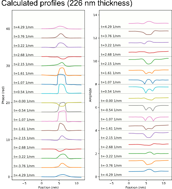
Since the holograms are recorded under strongly diffracting conditions, we additionally performed multislice image calculations for a wide range of incident beam tilts and specimen thicknesses. Strain relaxation effects at the specimen surfaces were included in the simulation by obtaining atomic displacements from finite element strain calculations for each simulated thickness. Profiles for a sweep of the incident beam direction for an exemplary thickness of 226 nm thickness are shown in Figure 3.
Based on the image calculations we discuss the robustness of various measures, which can be used for determination of the polarization field within the quantum well. For instance, the profiles in Figure 2 already show that the phase slope within the quantum well is not a very suitable measure for a possible field, since this slope is too sensitive to beam tilt. On the contrary, the step between the phase levels on both sides of the quantum well is robust measure for the potential difference across the quantum well. Together with the width of the well this step can be used to determine the polarization field inside.
Figure 1: Reconstructions of overview and detail holograms.
Figure 2: Experimental profiles across the bottom quantum (evaluated from the marked region of Figure 1) for various beam tilts. The phase profiles are normalized such, that the phase gradient between the quantum well is nullified.
Figure 3: Calculated profiles for a 226 nm thick specimen, no polarization fields were included in this calculation.
- References
[1] T. Takeuchi, et al., Japanese Journal of Applied Physics 36 (1997), L382.
[2] B. Haas, et al., Ultramicroscopy 198 (2019), 58.
[3] We thank D. Cooper for the providing us with the InGaN/GaN specimen.