Quantification and mitigation of electron-beam induced carbon contamination
- Abstract number
- 79
- Event
- Virtual Early Career European Microscopy Congress 2020
- Presentation Form
- Submitted Oral
- DOI
- 10.22443/rms.emc2020.79
- Corresponding Email
- [email protected]
- Session
- PST.6 - In-situ and in-operando microscopy
- Authors
- Milena Hugenschmidt (1, 2), Katharina Adrion (2), Dr. Erich Müller (1, 2), Prof. Dagmar Gerthsen (1, 2)
- Affiliations
-
1. 3DMM2O - Cluster of Excellence (EXC-2082/1 – 390761711), Karlsruhe Institute of Technology (KIT)
2. Laboratory for Electron Microscopy, Karlsruhe Institute of Technology (KIT)
- Keywords
carbon contamination, Helios G4 FX, low-keV-STEM, sample cleaning, TSEM
- Abstract text
Electron-beam induced carbon contamination is a daily issue in electron microscopy. The growth of contamination is unwanted because it worsens the lateral resolution by covering structures that are of interest. Although beam-induced carbon contamination is pervasive, astonishingly few studies deal with the quantitative analysis and the principles of contamination growth. Besides understanding of the growth mechanisms, the mitigation of carbon contamination is of interest. A variety of sample cleaning methods is available since it is believed that a significant fraction of contaminants are introduced by the sample itself. Another attempt to reduce contamination is to improve the vacuum in the sample chamber of the microscope. Hettler et al. [1] found that contamination growth is a diffusion-limited process at 300 keV in a transmission electron microscope. Mitchell [2] performed a detailed analysis of contamination mitigation strategies for 200 keV. Hirsch et al. [3] studied contamination in a scanning electron microscope and used a theoretical description of the effect by Müller [4]. However, a systematical and quantitative analysis of the dependence of contamination on parameters like primary electron energy, electron dose, and dose rate has not been performed up to now.
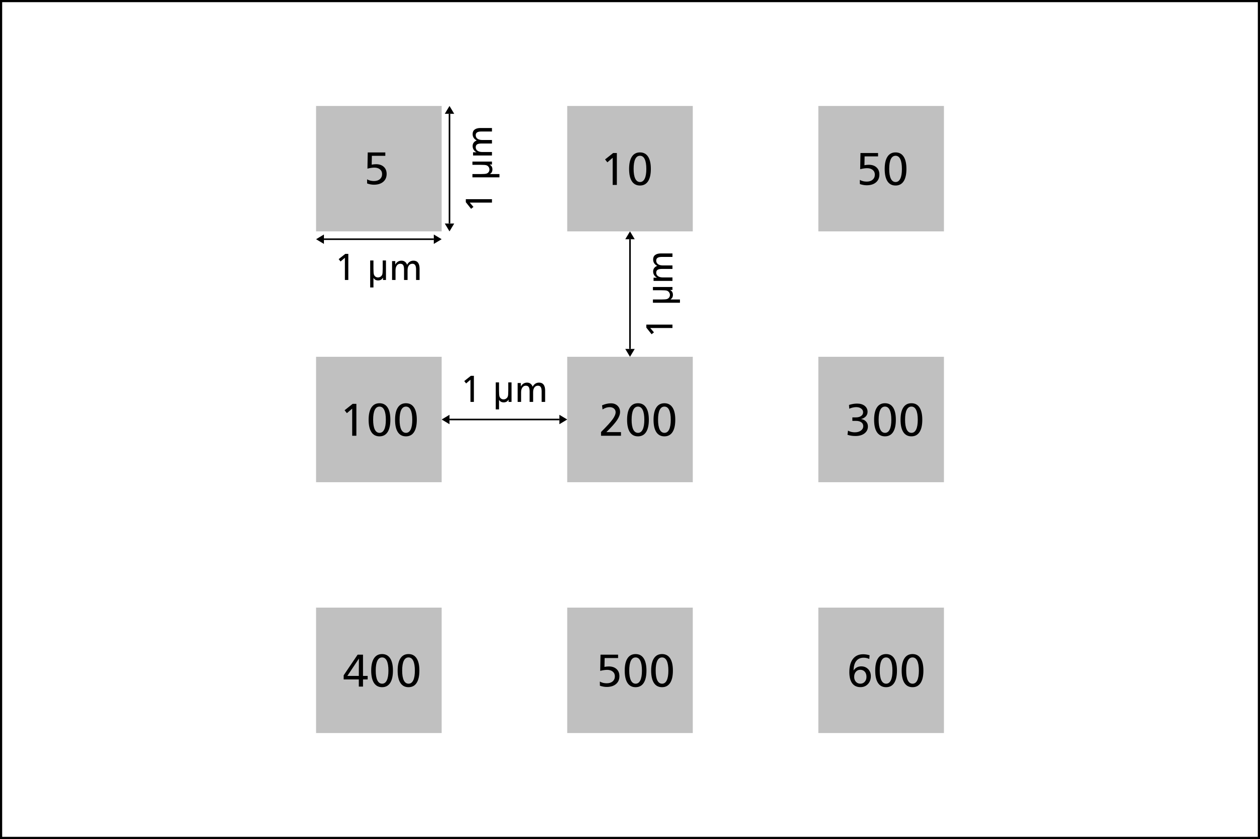
In this work, we have performed contamination studies in a Thermo Fisher Helios G4 FX at low electron energies between 0.5 and 30 keV. Thin (~10 nm) amorphous carbon films produced by adaptive carbon thread evaporation and placed on standard TEM-grids were used as test samples. Commercial carbon films showed irreproducible results due to different degrees of pre-contamination. Contamination was studied by scanning squares of 1x1 µm2 size for time periods between 5 and 600 s under reproducible conditions (cf. Fig. 1 for contamination pattern). In addition, primary electron energy, beam current, total dose and dose rate were varied to gain insight into the principles of contamination growth.
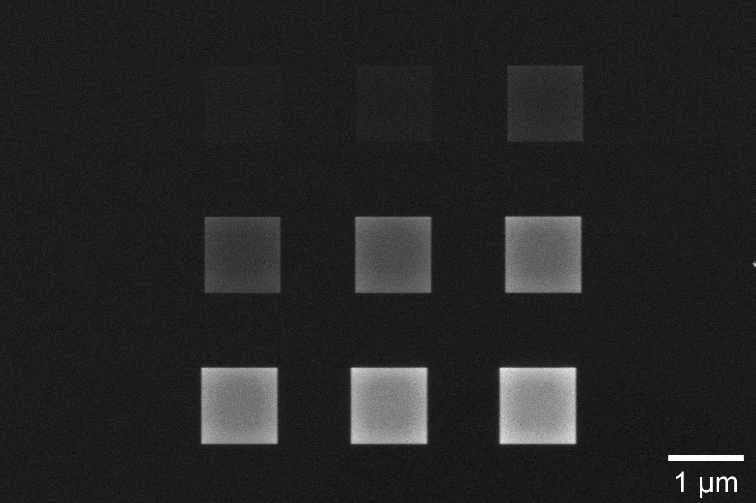
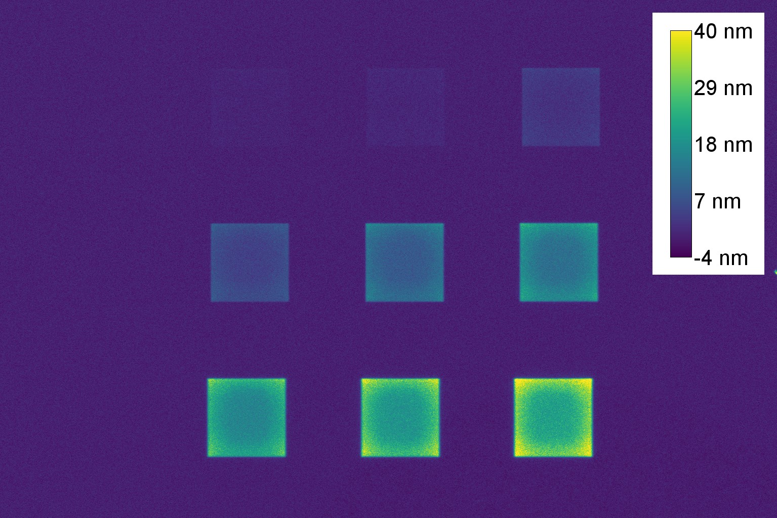
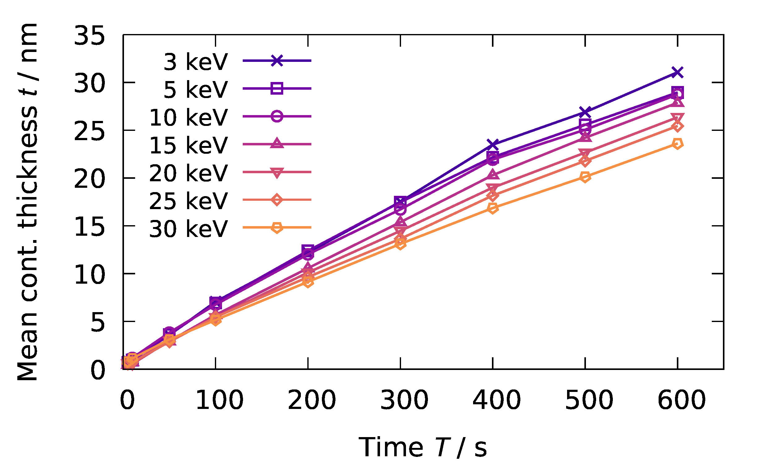
The contamination thickness was determined from high-angle annular dark-field scanning transmission electron microscopy (HAADF-STEM) images acquired in the same microscope. HAADF-STEM images (cf. Fig. 2) yield normalized intensities (normalization with respect to the intensity of the incident electron beam), which allow to extract the local thickness of the contamination patches by comparison with Monte Carlo simulations. An example of a thickness map is shown in Fig. 3. Averaging the thickness of each square yields average contamination thicknesses depending on the irradiation time. The dependence of the contamination thickness as a function of the scanning time is displayed in Fig. 4 for electron energies between 3 and 30 keV. As expected, the contamination thickness increases with scanning time without showing saturation in the investigated range. Contamination growth also depends strongly on the primary electron energy and is pronounced at lower energies. This effect can be qualitatively understood by the increase of the Bethe stopping power with decreasing primary electron energy [3]. Further results show that contamination is not a pure dose effect, but rather a diffusion-limited dose-rate effect.
The technique for measuring beam-induced carbon contamination that is suggested in this work, is appropriate to test the characteristics of contamination growth and sample cleaning methods. In the further course of this work, sample cleaning strategies will be tested concerning their efficiency.
Figure 1. Electron beam pattern. The numbers in the squares indicate the scan time in seconds. Figure 2. 20 keV-HAADF-STEM image of a contamination pattern grown at 15 keV. The contamination time increases from the upper left corner (5 s) to the lower right corner (600 s). Figure 3. Thickness map of contamination grown at 15 keV with subtracted average background thickness of the amorphous carbon film. Figure 4. Contamination thickness as a function of the scanning time for primary electron energy between 3 and 30 keV. Lines between data points are guides for the eye.
- References
[1] S Hettler et al., Micron 96 (2017), p. 38.
[2] DRG Mitchell, Micron 73 (2015), p. 36.
[3] P Hirsch et al., Scanning 16 (1993), p. 101.
[4] KH Müller, Optik 33 (1971), p. 296.
[5] We acknowledge funding by the Deutsche Forschungsgemeinschaft (DFG, German Research Foundation) under Germany’s Excellence Strategy – 2082/1 – 390761711. We thank the Carl Zeiss Foundation for financial support.