Quantitative electric field imaging in GaN-based heterostructures by DPC STEM
- Abstract number
- 566
- Event
- Virtual Early Career European Microscopy Congress 2020
- Presentation Form
- Submitted Poster
- DOI
- 10.22443/rms.emc2020.566
- Corresponding Email
- [email protected]
- Session
- PST.1 - Phase Microscopy
- Authors
- Satoko Toyama (1), Takehito Seki (1), Yuya Kanitani (2), Yoshihiro Kudo (2), Shigetaka Tomiya (2), Yuichi Ikuhara (1, 3), Naoya Shibata (1, 3)
- Affiliations
-
1. Institute of Engineering Innovation, School of Engineering, University of Tokyo
2. R&D center, Sony Corporation
3. Nanostructures Research Laboratory, Japan Fine Ceramics Center
- Keywords
DPC STEM, GaN, electric field imaging
- Abstract text
Local electromagnetic fields inside specimens can be directly observed in real-space at high spatial resolution by using differential phase contrast (DPC) imaging in scanning transmission electron microscopy (STEM). In DPC STEM, deflection of electron beam due to electromagnetic fields is detected by a segmented detector or pixelated detector placed on the bright field (BF) disk region. Using DPC STEM, electromagnetic field observation in materials has been successfully conducted, including direct imaging of electric fields in p-n junction and magnetic fields in Skyrmions [1]. However, as for heterointerfaces such as GaN-based semiconductor devices, intense diffraction contrast originated from strong interfacial strain hinders the quantitative observation of electromagnetic fields by S/TEM. In this study, we attempt to suppress diffraction contrast in the DPC STEM image of GaN/AlGaN interfaces and to quantify the polar electric fields and local carrier distribution in the vicinity of the heterointerfaces.
We prepared two specimens as model samples for DPC STEM experiments. One consists of c-plane GaN/Al0.14Ga0.86N multi heterointerfaces, which are used for ultraviolet light-emitting devices. The other is a c-plane GaN/Al0.35Ga0.65N single heterostructure, which is expected that high-density electrons are accumulated at GaN interface and used for high electron mobility transistor. Focused ion beam was used for preparing TEM samples. We imaged the polarization fields and carrier distribution in the heterointerfaces by DPC STEM using JEM-ARM300CF at 300 kV, equipped with a second-generation 16-segment detector (SAAF, JEOL Ltd.) and a JEM-ARM200CF-based TEM at 200 kV, in which a newly developed magnetic-field-free objective lens system is installed [2], equipped with a third-generation 40-segment detector (JEOL Ltd).
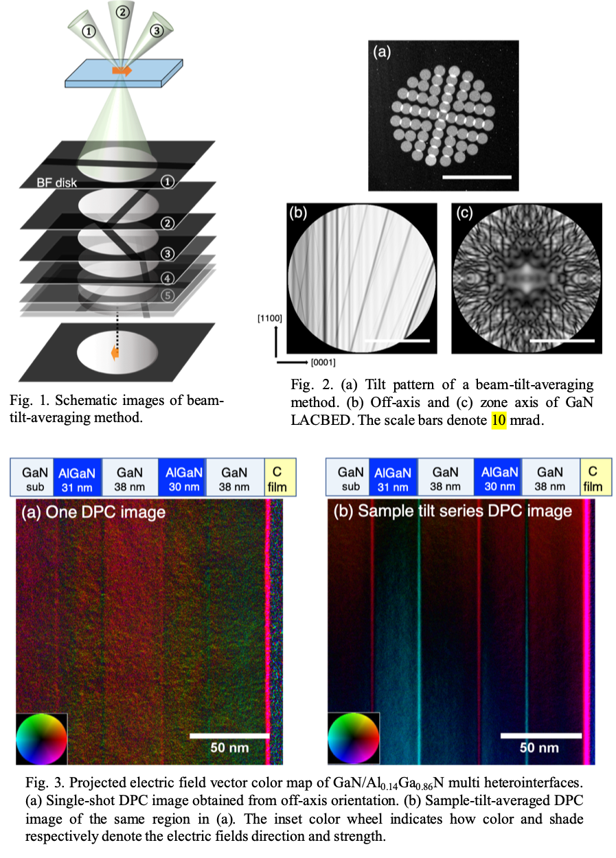
For reducing diffraction contrast in DPC images, we adopted the tilt-series acquisition method [3]. Bragg lines in the BF disks are very sensitive to the tilt condition of the specimen with respect to the incident beam direction, while the beam deflection by the electric fields inside the specimen should be insensitive to a slight difference in the sample tilt condition. Therefore, by averaging BF disks with various tilt conditions, it is expected that the diffraction contrast in DPC images can be suppressed and the electric field signals will remain in the DPC images (Fig.1). First, we acquired 264 DPC images with various sample tilt conditions from off-axis and then averaged those images for reducing diffraction contrast. Second, we used a beam tilt system and acquired the image with 60 tilt conditions around the zone-axis (Fig.2(a)). For evaluating error values in the specimen/beam-tilt-averaging experiments, large angle convergent beam electron diffraction (LACBED) patterns were calculated (Fig.2(b)(c)), and then BF disk patterns with the tilt-averaging were simulated. From the results of the experiments and the simulations, we confirmed the remaining diffraction contrast in the averaged DPC images is sufficiently weak to quantify electric fields in the heterostructures. As a result, polarization fields and local carrier distribution in GaN/AlGaN heterointerfaces can be experimentally acquired (Fig.3). The details of this method and evaluation of the results will be discussed in the presentation.
- References
[1] N. Shibata et al., Acc. Chem. Res., vol. 50, no. 7, pp. 1502–1512, 2017.
[2] N. Shibata et al., Nat. Commun., vol. 10, no. 1, p. 2308, 2019.
[3] A. Nakamura et al., Microsc. Microanal., vol. 23, no. S1, pp. 1412–1413, 2017.