Real-space cathodoluminescence imaging on an integrated correlative light and electron microscope
- Abstract number
- 1228
- Event
- European Microscopy Congress 2020
- DOI
- 10.22443/rms.emc2020.1228
- Corresponding Email
- [email protected]
- Session
- PST.6 - In-situ and in-operando microscopy
- Authors
- Amelia Liu (5), Alison Funston (1, 8), Gangcheng Yuan (1, 8), Timothy Davis (6), Joanne Etheridge (4, 7), Sangeetha Hari (2), Sabrina Rossberger (2), Lennard Voortman (3), Eric Piel (2), Toon Coenen (2)
- Affiliations
-
1. Centre of Excellence in Exciton Science, Monash University, Clayton
2. Delmic BV
3. Leiden University Medical Centre
4. Monash Centre for Electron Microscopy, Monash University, Clayton
5. School of Physics and Astronomy, Monash University, Clayton
6. School of Physics, University of Melbourne, Parkville
7. Department of Materials Engineering, Monash University, Clayton
8. School of Chemistry, Monash University, Clayton
- Keywords
cathodoluminescence
CLEM
correlative imaging
nanowire
nanophotonics
SEM
- Abstract text
In nanophotonics, nanoscale antennas, waveguides, and metasurfaces can be
used to confine, steer, and guide light within subwavelength volumes. Studying
the optical properties of such systems poses a major challenge owing to their
nanoscale dimensions, and as such, advancements in microscopy techniques are
required. Optical methods are limited in the excitation probe size and the spatial
resolution of the real-space image (both being approximately 300 nm).
Cathodoluminescence (CL) in the scanning electron microscope (SEM) has been
demonstrated to be an excellent nanoscale probe for analysing optically active
materials [1]. The focused electron probe acts as a local source of
electromagnetic fields that can excite both travelling waves and localized
resonant modes in nanoscale light-controlling systems. By scanning the electron
probe, maps of the optical excitability can be generated, showing the resonant
energy and direction of emission at each excitation point [1]. While this is a
powerful technique, detailed information about the point of emission of light
cannot normally be obtained. Some work has been performed on solar cell
materials using optical microscopy and NSOM by Haegel et al (see ref [2] for
overview).
Here, we demonstrate a novel alternative technique for measuring spatially
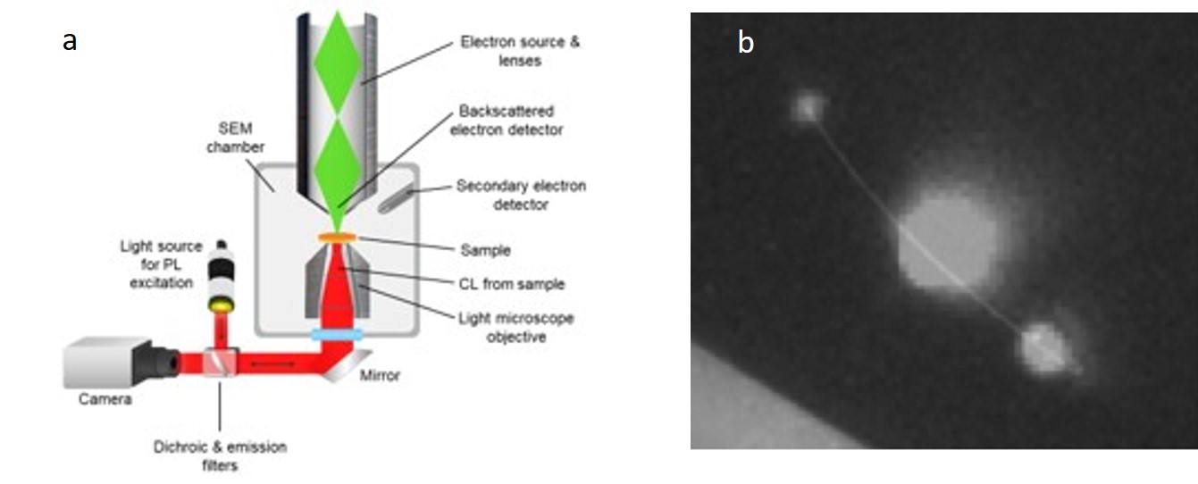
resolved CL, which has been developed in an integrated correlative light and
electron Microscope (a SECOM platform installed on a Thermo Fisher Verios 460
SEM). In this system (Fig. 1), light is collected below the sample using a high-NA
(0.95) microscope objective. The sample and objective can both be scanned
independently. The CL emission is directed towards an sCMOS detector which is
mounted on the outside of the SEM. In this system, the same optical
configuration can also be used to inject light, for correlative PL/CL
measurements, for example. The experimental workflow was implemented
using the open source control software (Odemis). The focussed electron probe
was scanned along a set of chemically synthesized silver nanowires dropcast on
a TEM membrane, with nanometer step size, exciting a travelling plasmon wave
which is coupled to the far field at the wire ends. A full-field, real-space image
of the light emission, superimposed on a high resolution SEM image, was
acquired for different electron beam excitation positions (Fig. 2), enabling the
detailed study of the plasmon propagation in the structure. This method has
many distinct advantages over measurements with an optical microscope. The
electron probe can excite guided plasmons at any point, unlike light which can
only couple in at the ends or at defects, as direct plasmon excitation is
momentum forbidden. In conjunction with spectroscopy and angle-resolved CL
imaging [1], a full understanding of excitability and emission in nanoscopic
optical materials can be obtained. We believe this novel experimental technique
has great potential to study scattering, light transport, and other diffusion
processes at the nanoscale for a variety of structures and materials.Fig. 1 Schematic of the integrated correlative light and electron microscope (the SECOM platform integrated on an SEM), showing the electron beam excitation of the sample, the CL collection scheme, as well as the light injection pathway for PL measurements (b) Real-space cathodoluminescence image of a silver nanowire, acquired for different electron beam excitation positions, superimposed on a high resolution SEM image, enabling the detailed study of plasmon propagation in the structure
- References
[1] Toon Coenen et al., MRS Bulletin, 40, 359 (2015)
[2]T. Coenen and N.M. Haegel, Appl. Phys. Rev. 4, 031103 (2017)