Scanning confocal electron diffraction (SCED): a method for nano-scale 4D-STEM at high angular resolution
- Abstract number
- 1389
- Event
- European Microscopy Congress 2020
- DOI
- 10.22443/rms.emc2020.1389
- Corresponding Email
- [email protected]
- Session
- PST.5 - Diffraction techniques and structural analysis
- Authors
- Dr. Mingjian Wu (1), Lilian Vogl (1), Prof. Dr. Erdmann Spiecker (1)
- Affiliations
-
1. Institute of Micro- and Nanostructure Research & Center for Nanoanalysis and Electron Microscopy (CENEM), Friedrich‐Alexander‐Universität Erlangen‐Nürnberg
- Keywords
4D-STEM, diffraction mapping, high angular resolution, crystallography, texture
- Abstract text
Diffractive mapping, or 4D-STEM, has gained rapidly increasing interest and has benefited many applications in the past years thanks to the developments of cameras and computer power and algorithm to handle large datasets. As STEM based methods, where the camera is recording the diffraction plane, which is conjugated to the probe defining aperture, the angular resolution is limited by the large size of condenser aperture. Even applying nano-beam optics setting (e.g. microprobe mode on ThermoFischer TEMs), the highest angular resolution (beam disk diameter) can only go down to around 1 mrad, which may limit certain applications. Here we propose a 4D-STEM method capable of mapping diffraction information of nano-scale samples at high angular resolution. The method is inspired by an earlier approach for high angular resolution ω-q patterns [1]. Since the optics setting is based on that of confocal microscopy, we call it scanning confocal electron diffraction (SCED).
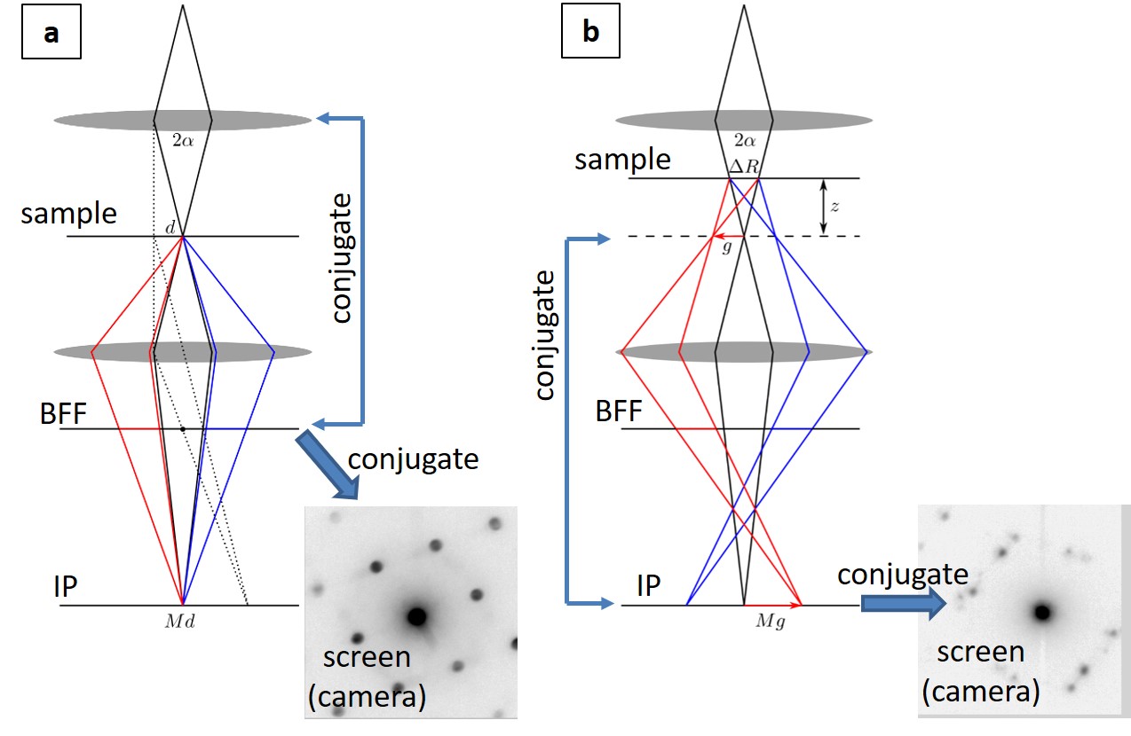
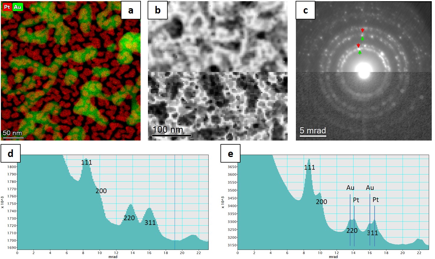
Figure 1 show the schematic beam path of STEM and SCED. In SCED, the screen/camera is recording the image plane instead of the diffraction plane like in STEM case. Diffraction information is introduced by raising the sample from the confocal plane by distance z. In this case, the spatial resolution is defined by the illumination circle ΔR of the probe, which is related to the convergence half angle α and z by a simple relation: ΔR = αz. The angular resolution θmin is defined by the probe size d and z: θmin = d/z = (0.61λ/α)/z. We have applied here small angle approximation and considered only small convergence angles where the probe size is limited by diffraction since the purpose is to balance spatial and angular resolution in the 4D datasets. Using 300keV electrons, 1 mrad beam convergence, and shifting the sample by 8 µm corresponds to a spatial resolution of 8 nm and angular resolution of 0.15 mrad. In order to demonstrate the high angular resolution of SCED, these parameters have been applied to a sample of Au and Pt nanoparticle (with difference in lattice constants Da/a » 4%) deposited on either side of a SiNx membrane, and compared the method with nanobeam diffraction mapping. The results are shown in Fig. 2. Radial separation of the Au and Pt diffraction spots is only possible to reveal in SCED. Since the full 4D data were recorded, more advanced analysis, e.g., virtual apertures, multi-variant statistical analysis, texture and nano-crystallography studies, can be applied computationally.
Figure 1. Schematic beam path of STEM (a) and SCED (b). Scanning coils and beam shift/tilt neglected in the scheme. Details see text.
Figure 2. (a) STEM-EDX mapping of the sample used to demonstrate and compare the methods. The sample is Au and Pt nanoparticles (lattice mismatch ~4%) deposited on either side of SiNx membrane. (b) Virtual bright-field image calculated from 100x100x1024x1024 4D datasets of (upper) SCED and (lower) scanning nanobeam diffraction (different sample area than shown in (a)). Spatial resolution of better than 10 nm is achievable by SCED. Experimental condition see text. (c) sum diffraction patterns of the 4D datasets from (upper) SCED and (lower) Scanning nanobeam diffraction. Azimuth integrated profile of the respective patterns are shown in (d) and (e). Separation of the Au and Pt rings is only possible in SCED.
- References
[1] P.A. Midgley, Ultramicroscopy 76 (1999), pp. 91.
[2] The authors gratefully thank the German Research Foundation (DFG) for financial support within the frameworks of the research training group GRK1896 “In situ Microscopy with Electrons, X-rays and Scanning Probes” and SFB953 “Synthetic Carbon Allotropes”.