TEM based investigation of strategies towards monolithic integration of Germanium on Silicon
- Abstract number
- 564
- Event
- European Microscopy Congress 2020
- DOI
- 10.22443/rms.emc2020.564
- Session
- PSA.3 - Semiconductors & Devices
- Authors
- Christoph Flathmann (1), Yvo Barnscheidt (2), Hannah Genath (2), Tobias Meyer (1), Hans-Jörg Osten (2, 3), Michael Seibt (1)
- Affiliations
-
1. 4th Physical Institute – Solids and Nanostructures, University of Goettingen, Friedrich-Hund-Platz 1, 37077
2. Institute of Electronic Materials and Devices, Leibniz University Hannover, Schneiderberg 32, 30167
3. Laboratory of Nano and Quantum Engineering, Leibniz University Hannover, Schneiderberg 39, 30167
- Keywords
4D-STEM Bragg measurements, Carbon mediated epitaxy, In situ TEM, Monolithic integration, Patterned probe, Strain mapping
- Abstract text
For integration of thin Ge layers on Si substrates, special growth strategies are needed to obtain films with the desired properties such as tailored dislocation densities and degree of strain relaxation on a nm scale. Information about both are obtainable with different TEM methods. In this work, threading dislocations are characterized in Ge layers grown by carbon mediated epitaxy. Moreover, in situ heating TEM is utilized to analyze dislocation behavior during annealing. Finally, patterned probe 4D-STEM Bragg measurements are performed for strain mapping in differently grown Ge layers.
Due to its higher charge carrier mobility and smaller bandgap compared to Si, Ge is an interesting material for channel materials and photonic devices. For instance, Ge based photodetectors [1] and lasers [2] have already been successfully realized. For integrated circuit applications, however, fully relaxed and smooth thin Ge layers with low dislocation densities are beneficial. Unfortunately, fully relaxed and smooth Ge layers usually exhibit high dislocation densities. Therefore, special growth strategies are needed to optimize the quality of thin Ge layers on Si.
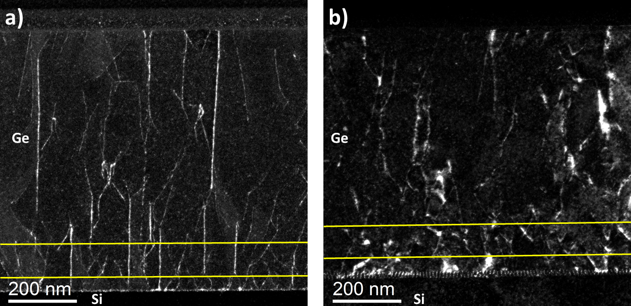
One strategy is carbon mediated epitaxy (CME) [3,4]. In this process, a thin Ge layer is deposited on Si at low temperatures. This is followed by deposition of a sub monolayer of carbon and a subsequent annealing step. As a result, edge dislocations are formed and fully relaxed and smooth Ge layers with thicknesses as low as 20 nm can be obtained [5]. By integration of additional carbon layers during further Ge growth, reduction of threading dislocations can be achieved based on the strained layer superlattice concept [6,7]. As can be seen in the weak beam dark field images in Figure 1, the lattice mismatch is accommodated in the bottom layer via misfit dislocations. Furthermore, bending and loop formation of threading dislocations at the carbon layer can be observed. In order to understand the underlying mechanism, annealing is carried out using in situ heating TEM. Hence, changes of the dislocations can be observed and directly correlated with the corresponding temperature.
As the detailed strain relaxation in such stacks is important for device quality, the capability of TEM to quantitatively map strain with nm spatial resolution needs to be exploited. Therefore, the recently developed method of patterned probe 4D-STEM Bragg measurements is applied [8,9]. Strain is mapped for two differently grown samples, i.e. (i) for Ge layers, grown with the previously described CME process, before and after annealing, and (ii) a fully relaxed 40 nm SiGe layer, also grown with CME [10], capped with a 20 nm Ge layer. The results are compared to x-ray diffraction measurements which indicate pseudomorphic strain of 1% in the Ge layers.
In conclusion, this work highlights the capabilities of modern TEM methods to characterize growth techniques for thin films. Advanced TEM methods, such as in situ heating TEM and patterned probe 4D-STEM Bragg measurements, are used to better understand carbon mediated epitaxy. Even though this work is focused on strategies towards Ge monolithic integration, the TEM methods are applicable to a variety of similar problems.
Figure 1. Weak beam dark field images of Ge layers grown with carbon mediated epitaxy on Si(001). The carbon layers are marked with yellow lines. a) Shows a (004) weak beam dark field image, where loop formation at the carbon layer can be seen. b) Shows a (220) weak beam dark field image, where misfit dislocations at the Si/Ge interface can be seen.
- References
[1] J. Michel et al, Nature Photonics 4 (2010), 527-534.
[2] S. Wirths et al, Nature Photonics 9 (2015), 88-92.
[3] D. Tetzlaff et al, Appl. Phys. Lett. 100 (2012), 12108.
[4] D. Tetzlaff et al, J. Cryst. Growth 378 (2013), 254-258.
[5] Y. Barnscheidt et al, Semicond. Sci. Technol. 33 (2018), 104006.
[6] J. W. Matthews and A. E. Blakeslee, J. Cryst. Growth 27 (1974), 118-125.
[7] J. W. Matthews and A. E. Blakeslee, J. Cryst. Growth 32 (1976), 265-273.
[8] T. Grieb et al, Ultramicroscopy 190 (2018), 45-57.
[9] S. E. Zeltmann et al, Ultramicroscopy 209 (2020), 112890.
[10] H. Genath, J. Schmidt and H. J. Osten, J. Cryst. Growth 535 (2020), 125569.