TEM specimen-induced artefacts of quantifying the chemical composition of SiGe-based epitaxial structures by STEM-based EDXS
- Abstract number
- 607
- Event
- European Microscopy Congress 2020
- DOI
- 10.22443/rms.emc2020.607
- Corresponding Email
- [email protected]
- Session
- PST.4 - Spectroscopies in Electron, X-ray and Ion Microscopy
- Authors
- Holm Kirmse (1), Daniel Schwarz (2), Jörg Schulze (2), Christoph T. Koch (1)
- Affiliations
-
1. Humboldt-Universität zu Berlin, Institut für Physik, AG SEM Berlin
2. Universität Stuttgart, Institut für Halbleitertechnik
- Keywords
Energy dispersive X-ray spectroscopy
Quantification of chemical composition
Scanning TEM
SiGe on Ge
- Abstract text
Energy dispersive X-ray spectroscopy (EDXS) performed in a transmission electron microscope (TEM) provides access to the chemical composition of a material. The result of quantification strongly depends on the geometry of the TEM specimen. Parameters like specimen thickness at the position of analysis and its distance from adjacent material might alter the quantification. In this work we identify artefacts of EDXS-based quantification of chemical composition by means of cross check with independent transmission electron diffraction (TED) and how to suppress it by optimized TEM sample preparation.
Recently the behavior of Group IV elements as direct semiconductors raised great interest for monolithic integration of the laser light source on Si [1-2]. Here the ternary alloy SiGeSn is of particular interest due to its direct bandgap at specific chemical composition [3-6]. Furthermore, SiGeSn allows the decoupling of its lattice constant and bandgap which enables lattice-matched strain-reduced growth on Ge [6]. Of particular concern is therefore the chemical composition of SiGeSn and the crystal quality for the fabrication of optoelectronic devices. However, lattice matching and the ternary nature of the alloy hinder the determination of the alloy composition with standard methods like X-ray diffraction. Hence, there is an urgent need for precise quantification of the chemical composition of SiGeSn by EDXS. For this work the complexity is reduced by studying a binary SiGe layer first.
The sample was grown by molecular beam epitaxy on Si(001) comprising a 500 nm thick Ge layer and a 100 nm Si0.3Ge0.7 layer. The details of the growth process and temperature treatment and dopant profiling is described elsewhere [7].
TEM specimens were conventionally prepared in cross-section resulting in a wedge shape [8]. The preparation comprised mechanical pre-thinning and final Ar+ ion milling.
EDXS was performed in scanning TEM (STEM) mode at a JEOL 2200FS operated at 200 kV using a 30 mm2 Bruker silicon drift detector. The electron probe was 1 nm in diameter. Sum spectra of the individual layers were acquired from rectangular areas of 50 nm x 500 nm elongated parallel to the interfaces. The acquisition time for an integrated spectrum was 150 s. For systematic investigations spectra were acquired for three different specimen thicknesses as indicated by the mean count rate of 250 cps (thickness about 100 nm), 900 cps, and 1500 cps, respectively. The chemical composition was calculated using tabulated Cliff-Lorimer factors.
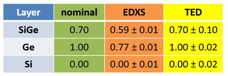
Additionally, TED was performed for areas of 500 nm in diameter with the individual interface centered within the selected area aperture. The TED measurement was calibrated using the Si substrate as standard. The chemical composition was calculated using linear Vegard´s law even considering potential tetragonal distortion of the unit cell.The Ge content xGe of the three components of the layer system i.e. Si substrate, Ge layer and SiGe layer was derived from both, EDXS and TED. The results are listed in Table 1. The nominal values are given for comparison. There is an obvious disagreement between the values derived from EDXS in comparison to the nominal values for both layers, Ge and SiGe. Against that, the values derived from TED perfectly agree with the nominal Ge content. Hence, artefacts have to be considered contributing to the EDXS measurement.
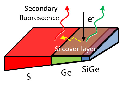
A first source of artefacts is the excitation of adjacent material by secondary fluorescence (Fig. 1). For this, the energy of X-rays excited in the region of interest (e.g. Ge-Kα) has to be higher than the energy of secondarily excited X-rays. This holds for Ge vs. Si with E(Ge-Kα) = 9.875 keV vs. E(Si-Kα) = 1.740 keV. Additionally, the Ge-Kα radiation has to access the Si substrate. This is highly probable since absorption of X-rays is negligible for distances shorter than 1 µm.
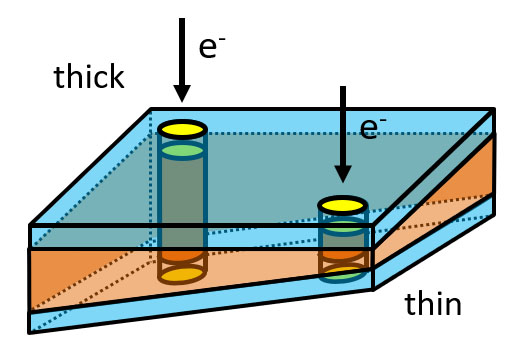
A second source of artefacts is a potential cover layer of foreign material on both sides of the specimen (Fig. 2). A cover layer can be caused by unintentional deposition during Ar+ ion milling. The altering of the measured chemical composition is significant for small specimen thickness and negligible for large specimen thickness.
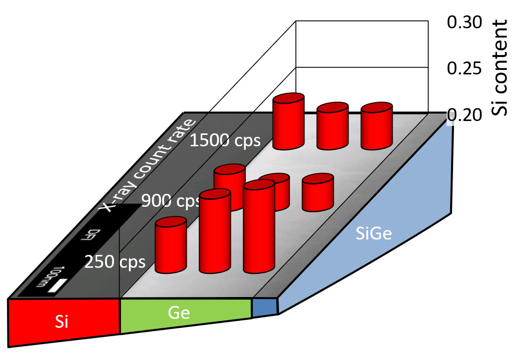
In order to discriminate between these two artefacts, the Si content of the Ge layer was determined in dependence on both, distance from the Si substrate and X-ray count rate representing specimen thickness (Fig. 3). For 900 cps and 1500 cps the Si content is almost constant with xSi = 0.23 with a slightly larger value of xSi = 0.24 when measured closer to the Si substrate. This hints to secondary fluorescence. Much more obvious is the increase of xSi to 0.29 for the thinnest region of the Ge layer (250 cps) where the TEM specimen thickness additionally decreases with distance from the Si\Ge interface. The increased xSi has to be attributed to a double-sided Si cover layer in favor of intermixed SiGe. For further insight in artefacts of EDXS, the results of EDXS measurements of a TEM specimen prepared by focused ion beam thinning will be discussed.Quantification of the chemical composition based on EDXS might become unreliable by artefacts owing to geometry and materials combination of the TEM specimen. In order to increase the reliability of the calculated chemical composition, cross-checking with independent methods like TED is indispensable.
Table 1: Ge content of the three different materials as revealed from EDXS and TED.
Figure 1: Sources of artefacts of EDXS due to geometry of the TEM specimen.
Figure 2: Contribution of a double-sided cover layer (blue) to EDXS of a homogeneous TEM specimen (orange).
Figure 3: Detected Si content of Ge layer vs. distance from Si\Ge interface and X-ray count rate representing specimen thickness.
- References
[1] S. Wirths et al., Nat. Photonics 9 (2015) p. 88.
[2] R. Koerner et al., IEEE 14th IC GFP (2017) p. 11.
[3] P. Moontragoon et al., J. Appl. Phys. 112 (2012) p. 073106.
[4] V.R.D´Costa et al., Thin Solid Films 518 (2010) p. 2531.
[5] S. Wirths et al., Thin Solid Films 557 (2014) p. 183.
[6] T. Wendav et al., Appl. Phys. Lett. 108 (2016) p. 242104.
[7] D. Schwarz et al., in preparation.
[8] K. Elsner is thankfully acknowledged for TEM specimen preparation.