Ultra-fast nano-optics with a high brightness transmission electron microscope
- Abstract number
- 911
- Event
- European Microscopy Congress 2020
- DOI
- 10.22443/rms.emc2020.911
- Corresponding Email
- [email protected]
- Session
- PST.2 - Microscopy for the study of quantum effects and nano-optics
- Authors
- Sophie Meuret (1), Yves Auad (3), Luiz Tizei (3), H.C. Chang (2), Florent Houdellier (1), Mathieu Kociak (3), Arnaud Arbouet (1)
- Affiliations
-
1. CEMES/CNRS
2. Institute of Atomic and Molecular Sciences, Academia Sinica
3. Laboratoire de Physique des Solides, Paris Saclay
- Keywords
Time-Resolved Cathodoluminescence
Electron energy gain spectroscopy
NV center in Diamond
Time- resolved Transmission Electron Microscopy
- Abstract text
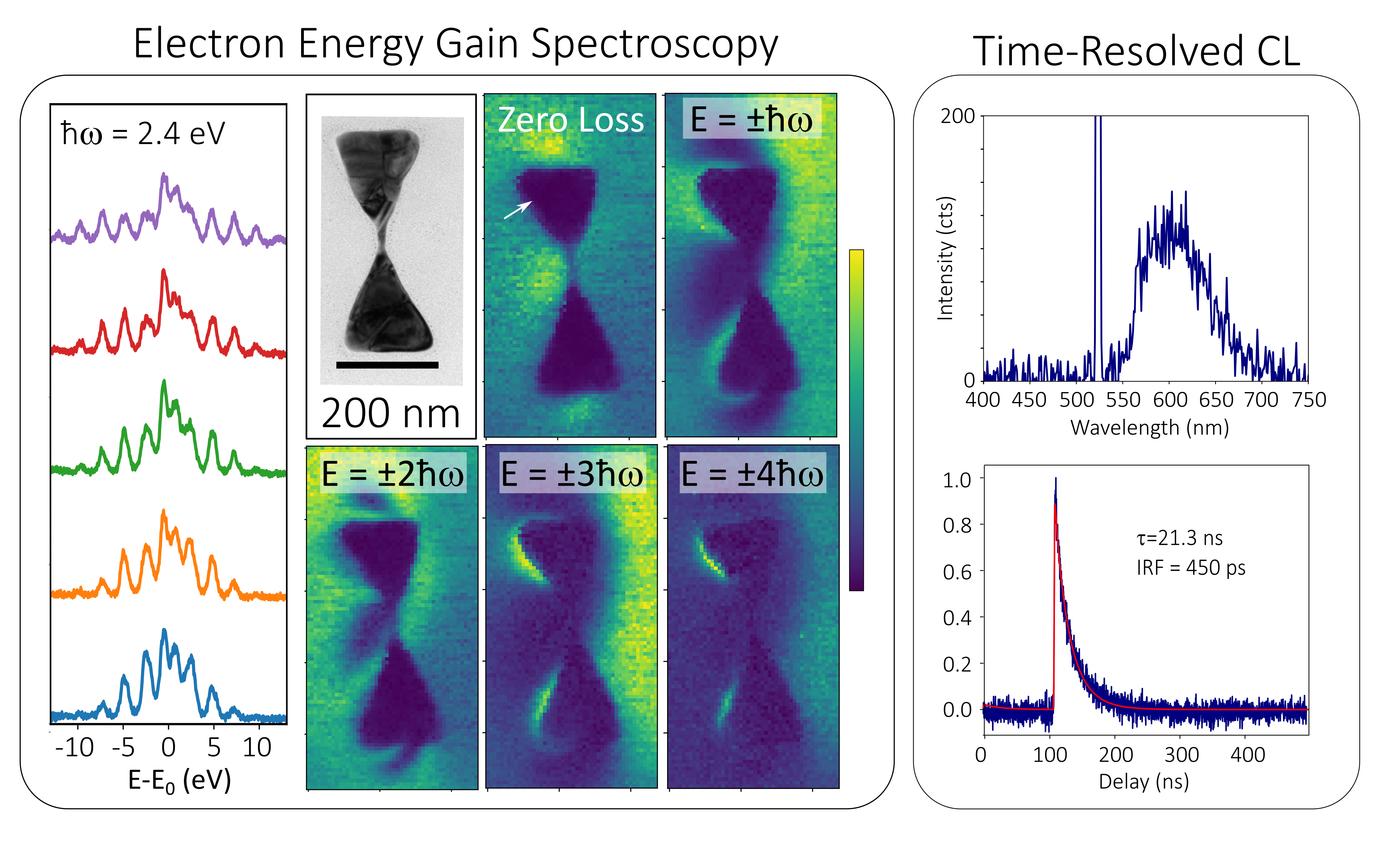
Nanoscale properties such as the shape of metallic nanoparticles or the atomic design of semiconductor heterostructures rule the emission and absorption of light by nano-structures. To overcome the diffraction limit of light (≈400 nm) one of the best techniques is electron microscopy. Indeed, the electron beam probes nano-objects with sub-nanometer resolution. Both Cathodoluminescence (CL) and electron energy loss spectroscopy (EELS) study the optical properties of nanostructures. They probe, for example, the luminescence properties for CL [1] and the local density of states for EELS [2]. Time-resolved electron microscopy is emerging since a decade, expanding the possibilities of these two techniques. In this presentation we will use a unique time-resolved transmission electron microscope based on a cold-FEG electron gun [3]. This technology allows, among other things, to reach a spatial resolution of 1 nanometer in pulsed mode. We will discuss the latest results of electron energy gain spectroscopy and the acquisition of the first cathodoluminescence decay traces in a transmission electron microscope (see Figure 1).
The coupling of a fast-electron with the near field created by the interaction of light with the nanostructure reveals light excitation patterns at the nanoscale. Using a pulsed transmission electron microscope, it is possible to simultaneously excite a nanostructure with both light and electrons. This pump-probe configuration allows the electron to couple to the optical near-field: it will either gain or lose quanta of energy from it [4]. Electron energy gain spectroscopy is the study of this phenomenon. The group of Zewail in Caltech did the first experimental study in 2009 [5]. Since then, a few groups reproduced and studied this effect, for example the group of C. Ropers showed quantum coherent manipulation of free-electron wave functions by their interaction with a confined light field [6]. In this presentation we will discuss electron gain spectroscopy using the first cold-FEG transmission electron gun [7]. This TEM allows the highest spatial resolution and highest brightness, leading to a spatial resolution of 1 nm and a strong interaction between the electron beam and the near field. Figure 1 shows a typical electron energy gain spectrum for a gold Bow Tie.
Cathodoluminescence spectroscopy is a powerful technique to study optical properties at the nanoscale. The light emitted by the sample after a local excitation by the electron beam is collected and can be analysed either with a spectrometer [8], [9] or an intensity interferometer [10], [11]. The first gives access to the spectral properties with a nanometer spatial resolution while the second measures the autocorrelation function of the cathodoluminescence signal (g(2)). The development of time resolved Cathodoluminescence (TR-CL) enabled the measurement of the lifetime of excited states in semiconductors with a sub-wavelength spatial resolution. It was used for example to measure the influence of stacking faults on the GaN exciton [12], to probe the role of a silver layer on the dynamics of a YAG crystal [13] or to show the influence of stress on the optical properties of ZnO nanowires [14]. Recently, the first pump-probe cathodoluminescence experiment using diamond revealed the effect of electron excitation on the nitrogen vacancy color center [15]. These results demonstrate that time-resolved cathodoluminescence is essential to study the correlation between semiconductor optical and structural properties (composition, defects, strain…). While all these pioneering studies were done using a scanning electron microscope, the improvement of the spatial resolution and the combination with other electron based spectroscopies offered by transmission electron microscopes will be a step forward for TR-CL. In this presentation, we will discuss the first time-resolved cathodoluminescence experiments within a transmission electron microscope. In this presentation we will discuss the first TR-CL results (see figure 1), and advantages and drawbacks of such a technology to perform TR-CL and pump-probe cathodoluminescence spectroscopy.
Figure 1 : Time Resolved spectroscopy in a Cold-FEG transmission electron microscope. Left: Electron energy gain spectroscopy on a Gold nano-Triangle. The laser (λ=515 nm) and the electron beam (E0 = 150 keV) excite the nanotriangle at the same time. Each spectrum is fitted to extract the different coupling orders, showing the pattern of near-field at the nanoscale determined by the angle between the incoming light and the nano-structure. Pixel size were 3 nm. Right: TR-CL of a NV center color defect of nanodiamond, the study was done at room temperature. The pic at 515 nm is the detection of the laser exciting the cold-FEG tip. The decay trace is the first taken in a TEM, after a fit we retrieve a lifetime of τe=21.3 ns, which is expected for a nano-diamond and an instrumental response function (IRF) of 450 ps due to the resolution of the detection apparatus.
In conclusion, this presentation will discuss the first results in EEGS and TR-CL using a unique Cold-FEG transmission electron microscope. Taking advantage of the high brightness and the 1 nm probe of the pulsed electron beam, we will present high spatial resolution maps revealing a strong coupling of the electron beam with the near field and the first decay trace acquisition in a TEM.
- References
[1] L. F. Zagonel et al., “Nanometer scale spectral imaging of quantum emitters in nanowires and its correlation to their atomically resolved structure,” Nano Lett., vol. 11, no. 2, pp. 568–573, 2011.
[2] A. Losquin et al., “Unveiling Nanometer Scale Extinction and Scattering Phenomena through Combined Electron Energy Loss Spectrosopy and Cathodoluminescence Measurement,” Nano-Letters, vol. 15, pp. 1229–1237, 2015.
[3] F. Houdellier, G. M. Caruso, S. Weber, M. Kociak, and A. Arbouet, “Development of a high brightness ultrafast Transmission Electron Microscope based on a laser-driven cold field emission source,” Ultramicroscopy, vol. 186, pp. 128–138, 2018.
[4] F. J. G. de Abajo and M. Kociak, “Probing the Photonic Local Density of States with Electron Energy Loss Spectroscopy,” Phys. Rev. Lett., vol. 100, no. 106804, 2008.
[5] B. Barwick, D. J. Flannigan, and A. H. Zewail, “Photon-induced near-field electron microscopy.,” Nature, vol. 462, no. 7275, pp. 902–6, Dec. 2009.
[6] A. Feist, K. E. Echternkamp, J. Schauss, S. V. Yalunin, S. Schafer, and C. Ropers, “Quantum coherent optical phase modulation in an ultrafast transmission electron microscope,” Nature, vol. 521, no. 7551, pp. 200–203, 2015.
[7] F. Houdellier, G. M. Caruso, S. Weber, M. Kociak, and A. Arbouet, “Development of a high brightness ultrafast Transmission Electron Microscope based on a laser-driven cold field emission source,” Ultramicroscopy, vol. 186, pp. 128–138, 2018.
[8] B. G. Yacobi and D. B. Holt, Cathodoluminescence Microscopy of Inorganic Solids. New York: Springer, 1990.
[9] L. F. Zagonel et al., “Nanometer scale spectral imaging of quantum emitters in nanowires and its correlation to their atomically resolved structure.,” Nano Lett., vol. 11, no. 2, pp. 568–73, Feb. 2011.
[10] L. H. G. Tizei and M. Kociak, “Spatially Resolved Quantum Nano-Optics of Single Photons Using an Electron Microscope,” Phys. Rev. Lett., vol. 110, no. 15, p. 153604, Apr. 2013.
[11] S. Meuret et al., “Photon Bunching in Cathodoluminescence,” Phys. Rev. Lett., vol. 114, no. 19, pp. 1–5, 2015.
[12] P. Corfdir et al., “Exciton localization on basal stacking faults in a-plane epitaxial lateral overgrown GaN grown by hydride vapor phase epitaxy,” J. Appl. Phys., vol. 105, no. 4, p. 043102, 2009.
[13] R. J. Moerland, I. G. C. Weppelman, M. W. H. Garming, P. Kruit, and J. P. Hoogenboom, “Time-resolved cathodoluminescence microscopy with sub-nanosecond beam blanking for direct evaluation of the local density of states,” Opt. Express, vol. 24, no. 21, p. 24760, 2016.
[14] X. Fu et al., “Exciton Drift in Semiconductors under Uniform Strain Gradients: Application to Bent ZnO Microwires,” ACS Nano, vol. 8, no. 4, pp. 3412–3420, 2014.
[15] M. Solà-Garcia, S. Meuret, T. Coenen, and A. Polman, “Electron-induced state conversion in diamond NV centers measured with pump-probe cathodoluminescence spectroscopy,” vol. 0, pp. 20–22, Oct. 2019.