Ultra-High Energy Resolution Electron Energy Loss Spectroscopy
- Abstract number
- 1194
- Event
- European Microscopy Congress 2020
- DOI
- 10.22443/rms.emc2020.1194
- Corresponding Email
- [email protected]
- Session
- PST.2 - Microscopy for the study of quantum effects and nano-optics
- Authors
- Dr Tracy Lovejoy (1), Dr Andreas Mittelberger (1), Chris Meyer (1), Dr Niklas Delly (1), Dr Matthew Hoffman (1), Dr Benjamin Plotkin-Swing (1), Dr Ondrej Krivanek (1, 2)
- Affiliations
-
1. Nion
2. Arizona State University
- Keywords
ultra-high energy resolution eels
angle-resolved EELS
vibrational spectroscopy
phonon dispersion
band dispersion
- Abstract text
The capability of vibrational spectroscopy in the electron microscope, introduced just 6 years ago [1], is growing rapidly. The Nion Iris spectrometer [2] incorporated into the Nion High Energy Resolution Monochromated EELS-STEM (HERMES™) system enables <5 meV energy resolution EELS in combination with atom-sized electron probes. Vibrational spectroscopy has already achieved:
- mapping with isotopic sensitivity, 13C vs 12C in an amino acid (L-alanine) at a specific carbon site, with ~30nm resolution [3]
- probing atomic vibrations at interfaces, and edges of nano-objects, with nm spatial resolution [4]
- 2 Å-level spatial resolution in the vibrational signal either in the dark-field geometry [5] or in an on-axis geometry in non-polar materials such as silicon [6]
- efficient mapping of acoustic and optical phonons in momentum space with nm spatial resolution using angle-resolved EELS [7]
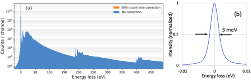
The HERMES system has recently attained 2.98 meV FWHM (full width at half-maximum) of the zero loss peak (ZLP) at 20kV. See Fig. 1b. The richness of vibrational spectra of complex materials, especially biological materials, is dramatically improved around 5 meV resolution compared to 8 meV [7], and further improvement in the capability of EELS is expected as the resolution improves.
A new generation of direct detectors is also expanding the capabilities of EELS. Figure 1a shows an EEL spectrum of boron nitride with 107 dynamic range in which an unsaturated zero loss peak is read out at the same time as inner shell loss edges, with 105 pA total beam current. The detector used here, Dectris ELA mounted on a Nion IRIS EELS as part of Nion HERMES microscope, has a large dynamic range, narrow point spread function, DQE(0) ~ 0.8 or better, and is resilient to radiation damage. It can detect up to 0.8 pA per pixel and hence a >100 pA EELS zero-loss peak (ZLP) without saturation, if the ZLP is spread over >125 pixels. At the same time, it can reliably detect isolated single electrons in the high loss region of the spectrum at the full speed of 2,250 frames/second with 16-bit resolution. There are 1030x514 pixels of 75um each,. The relationship between current and the raw detector counts becomes non-linear above 0.1 pA/pixel, but a ZLP count accurate to better than 1% is automatically recovered with count-rate correction, shown in orange. The detector uses a selectable threshold to exclude low energy events, and this results in essentially zero instrumental dark current and read noise. The high dynamic range and low noise of the new detector make it ideal for efficient parallel acquisition of angle-resolved EELS data where weak signals of interest exist very near to the intense ZLP.
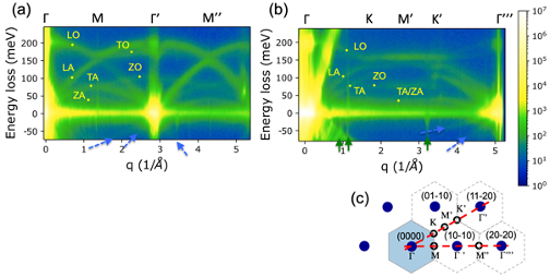
Figure 2 shows two angle-resolved EELS patterns, S(q,w), recorded from a hexagonal BN flake. The h-BN c-axis was parallel to the electron beam, and an EELS entrance slit selected scattering events along the directions in the diffraction pattern indicated in Fig. 2(c). Similar to S(q,w) patterns recorded with a scintillator-based SCMOS camera reported previously [7], the slit was 125 µm wide and 2.0 mm long. The diffraction patterns were rotated as needed using the post-sample lenses of the microscope column, whose principal effect at weak excitations is to rotate the beam. Other key parameters were as follows: Nion HERMES and Iris EELS, Dectris ELA hybrid-pixel direct detector, primary energy 60 keV, monochromator slit set to about 5 meV energy width, 4 pA beam current incident on the sample, incident beam convergence semi-angle ~2 mrad. For Fig. 2a, 240 separate exposures of 4 sec each were recorded and summed, for a total acquisition time of 16 min; for Fig. 2b, 120 exposures of 4 sec were summed (8 min total). The whole patterns and individual columns were aligned in energy prior to the summation.
The dispersion branches have been labeled in accordance with theoretical simulations of Senga et al. [ref. 8, extended data Fig. 4], with which they show excellent correspondence. ZLP tails have been suppressed to an extent that energy losses at energies as low as 30 meV are visible without performing any background subtraction, and energy gain dispersion branches, marked by dashed blue arrows, are readily distinguishable at room temperature.
The richness of the information available in Fig. 2 is striking, especially when it is compared to similar S(q,w) patterns acquired previously with much longer acquisition time. The patterns were recorded with a beam about 2 nm in diameter, as sub-unit cell spatial resolution is not compatible with good angular resolution. Similar data should be obtainable at stacking faults, grain boundaries and other defects in many types of materials, leading to a local analysis of vibrational properties not possible by any other experimental technique.
The fast-growing capability of ultra-high energy resolution EELS ensures a bright future for this field.
Figure 1. (a) EELS of hexagonal boron nitride with E0 = 60 keV, beam current = 105 pA, 100s exposure, α/2=27 mrad, β/2 = 50 mrad. and 0.5 eV/channel. This is raw data with no dark subtraction or gain normalization. (b) ZLP with 2.98 meV FWHM acquired at 20kV (333 x 3ms, a/2=b/2=15 mrad, 0.125meV/ch.).
Figure 2. (a) Experimental S(q,w) pattern of BN along the G-M-G’-M”-G”’ line. (b) S(q,w) pattern along G-K-M’-K’-G”. Dashed blue arrows indicate energy gain branches, short green arrows show artifacts due to slit charging. (c) Schematic diffraction pattern showing the first Brillouin zone (blue hexagon), higher order Brillouin zones, high-symmetry points in k-space, and the selection made by the EELS entrance slot. Nion HERMES, ELA direct detector, 60 keV.
- References
[1] O.L. Krivanek et al., Nature 514 (2014) 209; T. Miata et al., Microscopy 63 (2014) 377
[2] T.C. Lovejoy et al., Microsc. Microanal. 24 (Suppl 1, 2018) 446-447
[3] J. Hachtel et al., Science 363 (2019) 525–528
[4] MJ Lagos and PE Batson, Nature, 543, 529-532(2017), C. Dwyer et al., Phys. Rev. Lett 117 (2016) 256101
[5] F.S. Hage et al., Phys. Rev. Lett 122 (2019) 016103
[6] K. Venkatraman et al., Nat. Phys. 15, 1237-1241(2019)
[7] T.C. Lovejoy et al., Microsc. Microanal. 25 (Suppl 2, 2019) 628-629, and these proceedings
[8] R. Senga et al., Nature 573, (2019) 247.