Understanding atomic reconstruction in twisted transition metal dichalcogenides by STEM
- Abstract number
- 976
- Event
- European Microscopy Congress 2020
- DOI
- 10.22443/rms.emc2020.976
- Corresponding Email
- [email protected]
- Session
- PSA.1 - 1D & 2D Materials
- Authors
- Dr Yi-Chao Zou (1), Miss Astrid Weston (1), Dr Nicholas Clark (1), Dr Vladimir Enaldiev (1), Dr Alex Summerfield (1), Mr David Hopkinson (1), Prof Vladimir Fal’ko (1), Dr Roman Gorbachev (1), Prof. Sarah Haigh (1)
- Affiliations
-
1. University of Manchester
- Keywords
scanning transmission electron microscopy, 2D materials, physical science, atomic resolution, materials science
- Abstract text
Van der Waals (vdW) heterostructures are a unique class of layered artificial solids that offers the possibility of manipulating their physical properties via controlled material components, stacking order and relative rotation of adjacent atomic layers. When stacking a monolayer vdW material on top of another with a small-angle twist, the interlayer coupling between these two monolayers can induce an incommensure-to-commensurate transition at the interface (referred to as ‘atomic reconstruction’). Moiré superlattices in small angle twisted bilayer graphene have been shown to have superconductivity [1] and helical networks of topological edge states [2]. Significant breakthroughs have also been achieved in observing new physics in transition metal dichalcogenide (TMD) twisted bilayers, for example, localisation of excitons by stacking-dependent bandgap has been observed in WSe2/MoSe2 [3]. However, an atomic scale understanding of such reconstruction behaviour was still lacking in experiment. Here, we have investigated the lattice reconstruction in twisted MoS2 and WS2 bilayers, using atomic-resolution scanning transmission electron microscopy (STEM). The results are further interpreted in combination with results from density functional theory and conductive atomic force microscopy.
For the fabrication of STEM specimens, we start with making twisted bilayer TMDs using a remotely controlled micromanipulation transfer rig placed inside an argon atmosphere. Monolayer TMD flakes with crystallographic edges were prepared by mechanically exfoliating crystals onto Si/SiO2 that had been spin coated in polypropylene carbonate. A poly-methyl methacrylatecarrier (PMMA) layer was used to selectively pick up one flake (at 55 oC) followed by the other flake. To generate a small-angle twisted moiré superlattice, the transfer stage was rotated to angles close to 0o in a parallel (P) or 180o in an antiparallel (AP) configuration between flake pickups. A PMMA carrier layer was used to suspend the bilayer over a home-made holey SiNx membrane, which was removed by washing in a bath of acetone followed by isopropanol and hexane.
STEM imaging was performed using a probe-side corrected FEI Titan G2 80-200 S/TEM ChemiSTEM microscope and a JEOL ARM300CF double aberration corrected microscope with a cold FEG electron source. For high resolution annular dark field (ADF) imaging, the Titan was operated at 200 kV with a probe current of 40 pA, a 21 mrad convergence semi-angle, a 48-191 mrad ADF collection angle. The JEOL ARM300CF was operated at an accelerating voltage of 80 kV, with a beam convergence semi-angle of 31 mrad, probe current of 10 pA and an ADF collection angle of 68-206 mrad. High contrast images revealing overview of the moiré domains were achieved with a convergence angle of 6-7 mrad and an ADF collection angle range of 14-85 mrad, using either the Titan or JEOL microscope as mentioned.
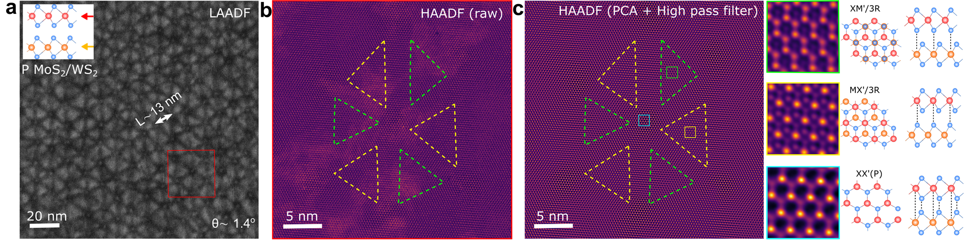
For imaging atomic reconstruction, we have developed a 3-step STEM protocol. (1) We first map the distribution and shape of the moiré domains on a nanometre to micrometre scale using low angle ADF (LAADF). This domain map is used as the navigation image to find the regions of interest (Fig. 1a). (2) We zoom into the regions of interest by changing to a large convergence angle with high-angle ADF (HAADF) imaging, so that atomic-resolution with interpretable atomic-number contrast can be achieved (Fig.1b). (3) For post image filtering, we applied principle component analysis (PCA) to denoise the images, as well as high pass filtering to reduce the intensity variation caused by surface hydrocarbon contamination left over from the flake transfer process (Fig. 1c).
The distribution and shape of the moiré domains is clearly seen from the diffraction contrast in LAADF image Fig. 1a. A small deviation (twist angle θ) from a perfect alignment gives rise to a moiré pattern with a period L = a/[2sin(θ/2)], with ,a, being the in-plane lattice constant, 0.32 nm. For Fig. 1a, L can be measured as ~13 nm and θ is deduced as ~1.4o. For P alignment, we observe triangular domains with boundaries visible as thin lines of darker contrast. High resolution images (Fig. 1b,c) show that the triangular domains are dominated by 3R stacking (marked by yellow and green triangles). In the 3R polytype of TMDs, chalcogenide atoms are aligned with the empty centres of the hexagonal rings in the layers above and below (right panel of Fig. 1c). We also investigated the atomic structure of AP aligned TMD bilayers with the effect of twist angle [4], where we consistently observe a kagome-like pattern dominated by 2H stacking when θ is close to 1o.
Fig. 1 (a) Low mag LAADF image showing periodic arrays of moiré domains in a ~1.4o twisted MoS2/WS2 bilayer. Atomic schematics inset illustrates parallel alignment of the two monolayers. (b) High resolution HAADF images zoomed into the region marked by red square in 1a. (c) Corresponding filtered high-resolution HAADF image (left panel), middle panel showing the images zoomed into local domains marked by yellow, green and blue squares. Right panel shows the corresponding atomic models. Red and orange balls denote the metal atoms (M: W, Mo) in the top and bottom monolayer respectively. Blue balls denote the chalcogenide atoms (X: S).
The lattice reconstruction for parallel aligned TMD bilayers creates condition for the formation of sizeable domains of 3R stacking (which is rarely found in natural MoS2 and WS2 where 2H stacking dominates), and features intrinsic asymmetry of electronic wavefunctions which can be used for electrical tuning of the optical properties of such twisted bilayers by a displacement field.
- References
1. Cao, Y., Fatemi V. et al. Unconventional superconductivity in magic-angle graphene superlattices. Nature 556, 43–50 (2018).
2. Yin, L. J., Jiang, H. et al. Direct imaging of topological edge states at a bilayer graphene domain wall. Nature Communications 7, 1–6 (2016).
3. Seyler, K. L. Rivera P. et al. Signatures of moiré-trapped valley excitons in MoSe2 /WSe2 heterobilayers. Nature 567, 66–70 (2019).
4. Weston A., Zou Y. et al. Atomic reconstruction in twisted bilayers of transition metal dichalcogenides. Nature Nanotechnology. Just Accepted (2020).