Understanding point defects in resistive switching of SrTiO3 by transmission electron microscopy
- Abstract number
- 1333
- Event
- European Microscopy Congress 2020
- DOI
- 10.22443/rms.emc2020.1333
- Corresponding Email
- [email protected]
- Session
- PSA.3 - Semiconductors & Devices
- Authors
- Dr. Tobias Schulz (2), Dr Toni Markurt (2), Thilo Remmele (2), Aykut Baki (2), Dr Joel Varley (1), Dr. Jutta Schwarzkopf (2), Dr Martin Albrecht (2)
- Affiliations
-
1. Lawrence Livermoore National Laboratory
2. Leibniz-Institut für Kristallzüchtung
- Keywords
SrTiO3, resistive switching, point defects, DFT, image simulation, transmission electron microscopy
- Abstract text
Recent work in oxide electronics suggests that understanding point defects in oxides could be the key to establish adaptive electronics at the device level. The paradigm of adaptive electronics is to create systems that are able to learn and to adapt to various inputs, i.e. to mimic human brain function. The most promising device for such applications with respect to technological needs in terms of scalability and capability, is the “memristor”: A passive two terminal device, that can be freely programmed into a high resistance state (HRS, or OFF state) or a low resistance state (LRS, or ON state) under external electrical stimuli. Among numerous other compounds, resistive switching has been observed in SrTiO3. A common model to explain this behavior is based on formation of a filament consisting of oxygen vacancies that open or close an electrically conductive channel by diffusion.
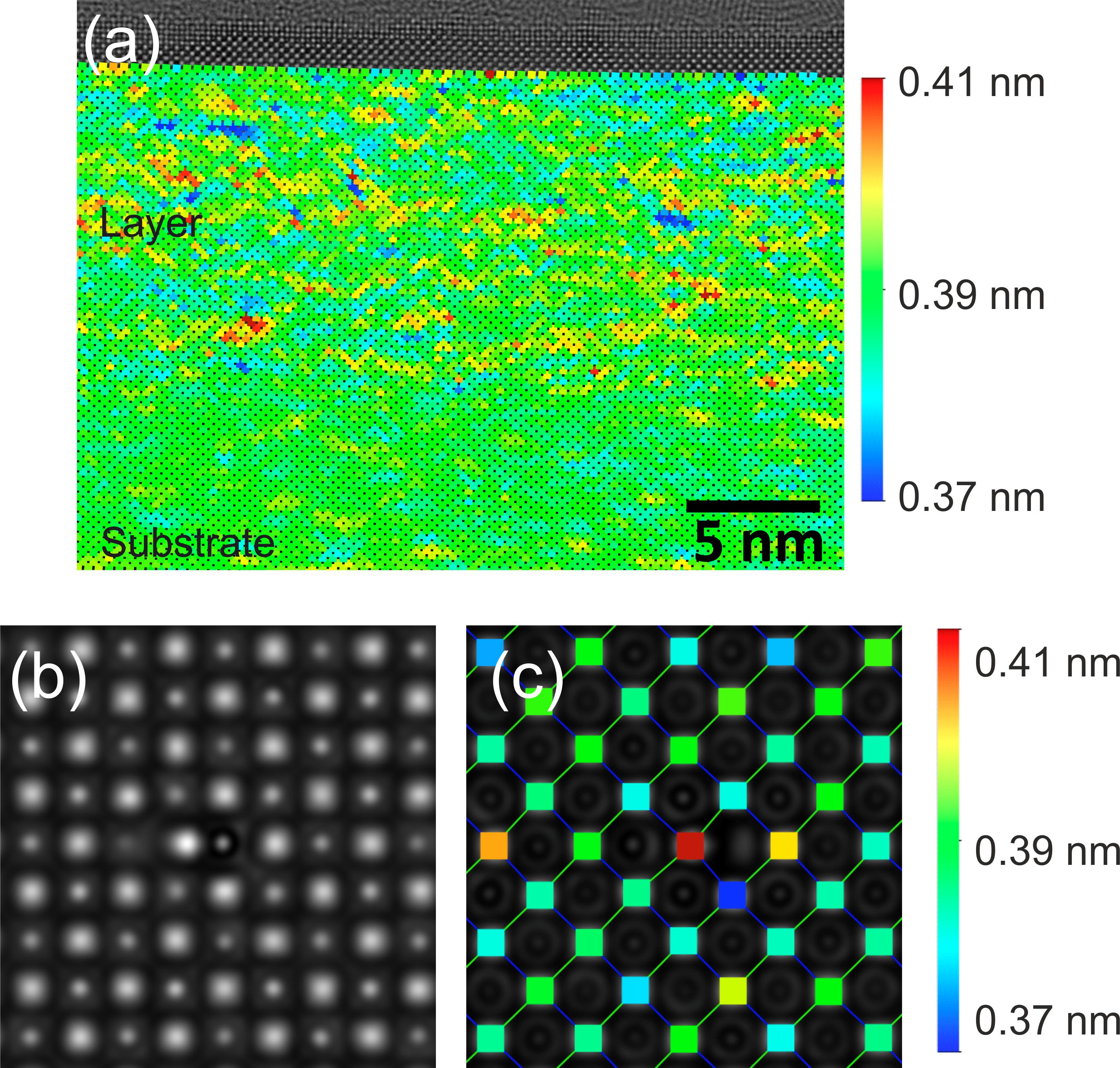
In this contribution, we show that resistive switching can be obtained formingless in SrTiO3 if the samples are grown under Sr deficiency. Combining electrical measuring techniques with transmission electron microscopy (TEM) and scanning TEM annular dark field (ADF), we propose that Ti antisites (TiSr) are responsible for the switching behavior. We consider defect assisted tunneling electroresitance in a ferroelectric tunnel junction as the underlying mechanism that causes resistive switching. Epitaxial SrTiO3 layers with controlled stoichiometry from Sr poor to stoichiometric were grown by metal organic vapor phase epitaxy (MOVPE) onto native SrTiO3:Nb substrates. To identify the relevant defect, we use aberration corrected TEM and scanning TEM-high angle annular dark field (HAADF) and low angle annular dark field (LAADF). While HAADF quantifies the stoichiometry, LAADF reveals local lattice distortions due to point defects causing diffuse scattering of the beam. TEM image simulations are performed using supercells consisting VO and TiSr with various concentrations based on density functional theory (DFT) calculations. Our electrical measurements show that layers grow under Sr poor conditions exhibit formingless resistive switching. TEM investigations of such layers reveal the following results: (i) A lower HAADF intensity is found in the Sr deficient layer as compared to the stochiometric substrate. (ii) According to energy dispersive s-ray (EDX) Sr deficiencies of up to 15% are confirmed. (iii) An increased LAADF intensity is observed in the layer as compared to the substrate, which is indicative for strong local strain fluctuations. (iv) Mapping the lattice spacing by a peak finding algorithm in TEM images reveals stronger local lattice distortions in the layer as compared to the substrate, as can be seen in Fig 1(a). This supports our STEM-LAADF results. (vi) Comparing the measured spacings between intensity maxima from image to image in a series of TEM images (acquisition time 100 ms) reveals stronger variations in the layer as compared to the substrate. From that, we conclude that the maxima and thus the positions of the respective atomic columns are subject to stronger position fluctuations, during recording the series.By comparing the above described experimental data with TEM image simulations of point defects, we conclude that our observations can best be explained by TiSr anitisite defect. Fig 1(b) shows an image simulation of the TiSr antisite defect for a sample thickness of 11 nm, which compared our experimental images. (i) Mapping the spacing between neighboring intensity maxima in our TEM simulations reveals fluctuations of the lattice in the region of the defect up to 7 % from the mean value, see Fig 1(c). This compares to the measured lattice distortions in the TEM images in Fig 1(a). (ii) Comparable to our experimental findings, STEM-HAADF (LAADF) image simulations of this defect reveals a lower (higher) intensity, as compared to a stoichiometric SrTiO3 case. (iii) With regard to the fluctuations of the position fluctuations of the atomic columns from image to image, we propose that this behavior stems from the varying orientation of the ferroelectric domain, induced by the VSr-Ti defect, during acquisition of the image series: TEM image simulation of various orientations of the ferroelectric domain support this attribution. The energy for these transitions could be provided by the electron beam of the microscope. STEM-electron energy loss spectroscopy measurements are currently pending to corroborate this assumption.
Fig 1(a) Lattice spacing map using by a peak finding algorithm in an experimental TEM image. (b) TEM image simulation of the SrTi antisite defect. (c) Lattice spacing map of the TEM image simulation in Fig 1(b).