Visualization of Nanostructures, obtained in the Process of ThermoplasmonicLaser-Induced Backside Wet Etching of Sapphire
- Abstract number
- 324
- Event
- European Microscopy Congress 2020
- DOI
- 10.22443/rms.emc2020.324
- Corresponding Email
- [email protected]
- Session
- PSA.5 - Nanoparticles & Catalysts
- Authors
- Prof. O.M. Zhigalina (1), Dr. D.N. Khmelenin (1), Ms. A.V. Atanova (1), Dr. N.V. Minaev (1), Prof. A.P. Sviridov (1), Dr. M.Yu. Tsvetkov (1)
- Affiliations
-
1. Federal Scientific Research Centre “Crystallography and Photonics” of the RAS
- Keywords
EDX mapping; Electron microscopy; Laser-induced backsidewet etching (LIBWE); Microstructuring; Nanoparticles; Plasmonics
- Abstract text
Laser-induced backside wet etching using water solution of plasmon precursor (AgNO3) as an absorbing medium provides effective structuring of such a complex material as sapphire. At the same time, this process is accompanied by the formation of silver nanoparticles and a significant modification of a surface layer of sapphire. Hybrid plasmon structures were formed on the surface of sapphire. The structure and phase composition of surface layer formed during the transformation of the materials in the process of etching have been studied using electron microscopy methods, electron diffraction, and EDX analysis.
A method of indirect impact of laser radiation on the materials was proposed in 1999 [1]. In this process, high-intensity laser radiation focuses on the back surface of a transparent dielectric, which is located in a cell filled with highly absorbing liquid. The developed version of this technology was called laser induced backside wet etching (LIBWE) [2]. This study examines the results of this approach, where a solution of plasmon precursor is used to create an absorbent medium. The implementable version of thermoplasmonic LIBWE (TP-LIBWE) provides etching of such difficult-to-process material as sapphire (as well as other promising optical materials such as glass, quartz, diamond). record etching speeds reaching several microns per pulse at energy densities ≤ 12 J/cm2 [3]. During this process, various phase transformations occur in the surface layer of sapphire; there is also significant modification of the materials, which is usually achieved only with femtosecond laser impacts. In addition, as a result of interaction with plasmon precursor, a thin layer. is formed, which allows considering the obtained structures in the context of the perspective of potential plasmonic applications.
The structure and phase composition of the obtained plasmon nanostructures have been studied by TEM, high resolution electron microscopy (HREM), and transmission scanning electron microscopy with z-contrast using a high-angle annular dark-field detector (HAADF STEM), electron diffraction, and EDX analysis (SuperX EDS system) in a FEI OSIRIS microscope with an accelerating voltage of 200 kV. For processing and analysing images and electron diffraction patterns obtained in an transmission electron microscope, Digital Micrograph, Esprit, TIA, and JEMS software were applied. TEM sample preparation was accomplished using a focused ion beam in a FEI Scios Dual Beam microscope.
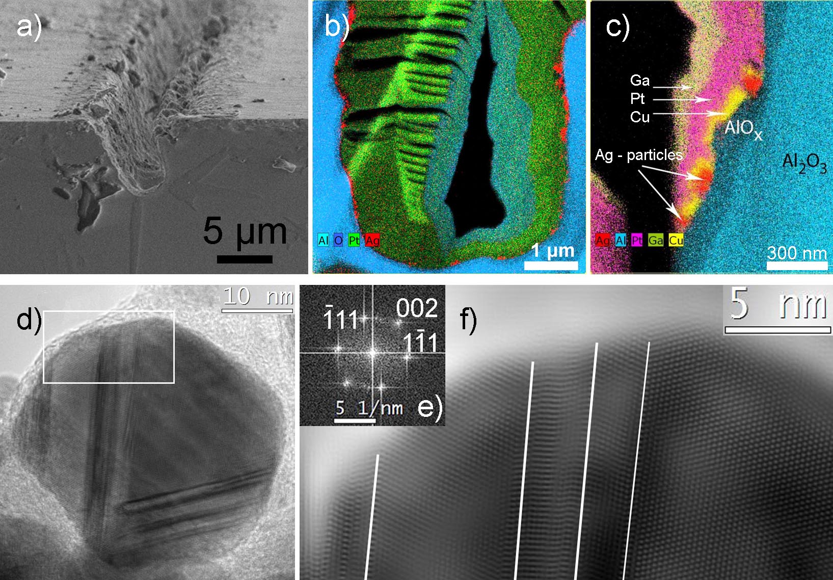
Microstructuring of such high-demand material as sapphire was carried out using thermoplasmonic laserinduced backside wet etching (TP-LIBWE). Electron microscopy and EDX mapping methods were used for studying the channels (Fig.1a,b) and hybrid plasmonic structures formed on the sapphire surface as a result of laser thermoplasmonic impact. It was established that under the influence of laser radiation, plasmonic precursor (AgNO3) is reduced to silver nanoparticles, which provide huge absorption of laser radiation. Due to this, a substantially localized area with extremely high temperatures and pressures providing sapphire ablation was formed in the absorbing solution—sample interface. It was shown that in this case, significant phase changes of the substance occurred: the amorphous phase with embedded silver nanoparticles was formed on the surface of the crystalline sapphire (Fig.1c). The thickness of the surface amorphous sapphire layer was up to 170 nm. The thickness of the layer with silver nanoparticles reached 50 nm; the size of nanoparticles varied in the range of 2-60 nm. The nanoparticles were located both in the amorphous layer and on its surface. It was established that the presence of twins was a characteristic feature of the nanoparticles observed (Fig. d,e).
Fig. 1. SEM image of sapphire with a channel obtained using LIBWE (a); an elemental map of the channel – a general view (c); an enlarged map with an amorphous layer and silver nanoparticles (d); HREM image of the Ag particle (e); enlarged filtered HREM image of the particle area highlighted by a white rectangle, white lines indicate twinning {111} planes (f); Fourier diffractogram taken from the particle area, the [110] zone axis (g).
- References
[1] J. Wang; H. Niino; A.Yabe Appl. Phys. A, 1999, 69, S271–S273.
[2] M.Yu.Tsvetkov; V.I. Yusupov; N.V Minaev.; P. S. Timashev; K. M. Golant; V. N. Bagratashvili. Laser Phys. Lett. 2016, 13, 106001.
[3] M.Yu. Tsvetkov; N.V. Minaev; A.A. Akovantseva; P.S. Timashev; A.E. Muslimov; V.M. Kanevskii. Quantum Electron, 2019, 49, 133-140.
[4] Electron microscopy investigations were carried out using equipment of the Shared Research Center of the Institute of Crystallography, Russian Academy of Sciences (project RFMEFI62119X0035) and was supported by Russian Foundation for Basic Research in part of the design of the laser facility (Grant No. 18-02-00420 A) and in part of the studies on sapphire etching processes (Grant No. 18-29-06056 MK).